We live in an age of abundant information. There is a tremendous exchange of ideas crisscrossing the world enabling new innovative type of products to pop up daily. Therefore, in this era there is a greater need to understand competitive intelligence. Corporate companies today are interested in what other competitors are brewing in their R&D labs and in predicting what novel application is coming up in the market so as to determine the best possible plan of action to counterattack. Moreover, new players with radically innovative ideas are rapidly emerging as partly deduced from the massive shift in the patent filing scenario in the past years. For example, in 2000, the three countries which filed the most patents were US, Japan and Germany. But since 2019, China has become the largest patent filing country with World Intellectual Property Organization (WIPO), surpassing USA, Japan, and Germany. South Korea has also emerged as a top five patent producers [1]. Companies around the world are looking for a synthesis of information from this data deluge. They are relying on industry experts to provide the technological know-how but also on patent engineers or analysts to perform the analysis of intellectual property (IP) of a particular company and/or a whole industry. Their aim is to understand the activities of the main players as well as the fields in which they dominate. Creating such a detailed patent landscape is time-consuming and complex, however, the end result could provide deep insights into the technology and the market.
I have come across several thorough patent landscapes that have predicted emerging technologies quite accurately. However, I have found mixed results for semiconductor road maps especially those related to advanced logic devices. Specifically, some of the major technologically break-through concepts in advanced logic devices were not predicted in time by market analysts or industry experts. The most striking example is the introduction of finFET device (a tri-gate where the gate wraps around the silicon fin for better control of the channel) by Intel in 2012 for its i5-3550 processor which arrived completely as a surprise to the industry.
The story gets even more interesting after the introduction of finFET devices. Very quickly there were multiple reports that after 10 nm node finFET devices were not going to be extendable. Solutions were proposed in public forums like IEEE papers, IEDM and VLSI conferences. Needless to say, prior to the publication of every proposed solution in a public literature, multiple patents related to them were filed by all major device manufacturers. All the patents and non-patent literature could be grouped into two categories: new materials or new device architectures. They discussed either new materials with existing technologies or suggested radical solutions where new device architectures were fabricated with new materials. For example, some of the serious propositions with prototype data were the following device structures: ultra-thin-body (UTB) field-effect-transistor (FET) based on silicon-on-insulator (SOI), gate-all-around (GAA) involving nano-wires/nano-sheets stacked horizontally or vertically, tunneling FET (TFET), and stacked FET. Meanwhile the materials section mainly focused on silicon -germanium (SiGe) replacing the silicon (Si) channel for PMOS or using III-V compounds. However, today, we are at 7 nm node and slowly transitioning to 5 nm node and still moving forward with the original finFET configuration.
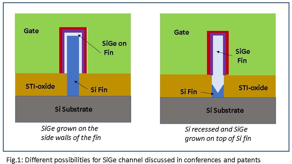
I wondered why these predictions were inaccurate and came to the following conclusions. Firstly, all these suggested devices in spite of their strengths had some serious concerns too. The ultra-thin-body (UTB) architecture gave the possibility of back biasing and also had low consumption of power. The initial wafer cost was high then. UTB is now not used but SOI based technology is currently widely prevalent in the market despite not being used in high speed processors. Similarly the GAA concepts provided better electrostatic control of the channel but required two materials which could be deposited one top of each other, each of them having a very different etch selectivity for the same etching chemistry. The onus on deposition and etching was high, which made the overall process flow very expensive. Vertical GAA FET devices which required major integration change as the wire-shaped channel regions were perpendicular to the substrate (implying that source and drain regions were not on the same plane) were especially hindered by their requirements. This implied additional process steps involving deposition and etching which would make the manufacturing of advanced logic devices even more expensive. Regarding TFET, there was the promise of attaining the sub-threshold slope limit of 55mV/dec, which could open new applications for low power computing. However, the band gap tunneling based TFET devices unfortunately lacked a robust drive current. Next, let us consider stacked FET devices. This idea had been floating since a long time in the technical forum. In this concept, transistors are stacked one on top of another. Either the transistors are made in separate wafers and bonded or they are fabricated directly on the lower layer of transistors. This requires good bonding techniques or proper controlling of the thermal budget for the top devices. Additionally, controlling the implant process could be difficult on the stacked layer. Back in 2012, the solutions were not ready. What about SiGe replacing Si? Most of the patents filed and literature submitted highlighted two possible scenarios both of which involved integration methods post fin formation. One requires growing SiGe on the side walls, while the other is recessing the fins between the isolation structures and growing SiGe on top of the fin (see figure 1). Both methods required at least additional mask sets and numerous process steps, which suggested that the end result would be expensive.

If you observe the track history of semiconductor manufacturers it becomes evident why none of these concepts ever made it into the mainstream. The continuous miniaturization or scaling of the devices has maintained the transistor count trend in accordance with Moore’s law even today [2]. The scaling is actually the shrinkage of all the dimensions of metal-oxide-semiconductor field effect transistor (MOSFET). Every time the semiconductor manufacturers were faced with process challenges or design difficulties due to scaling, they analyzed what is the smallest change that could be made in the integration scheme in order to continue to use the existing tool set and process flows in the new technology node. They also had to consider whether new processes that were to be introduced could be extended to future nodes. The strategy is that in every technology node when some new process-integration step is introduced, the majority of other process steps are kept unaltered. The direct result of this strategy is that with each coming generation the process-flow becomes more stable and reliable.
This strategy of minimum change for every new generation is well exemplified in Intel’s processors. Intel’s 22 nm had the 5th generation of strained silicon engineering with raised source-drain having embedded graded SiGe for PMOS channel, and embedded Si for NMOS. Similarly, for channel and gate engineering, high-k with replacement metal gates were introduced in 45 nm node and was further improved in 32 nm node and finally implemented in 22 nm finFET structure. Intel has maintained the same finFET architecture up to 10 nm. Yet the device performance has improved and the transistors per unit area count has increased. In the case of TSMC it is equally impressive, TSMC introduced finFET device at 16 nm node in the iPhone 7 processor in 2016, and since has produced three new generations of finFET devices. According to the press release, it will also continue to use finFET devices in their 5 nm devices [3].
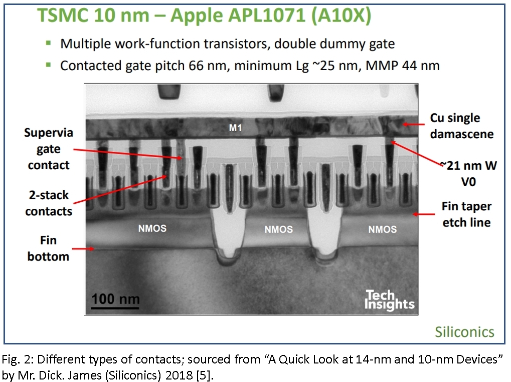
Needless to say the devil is in the details; detailed structural analyses are needed to understand the process evolution. Even though finFET configuration has remained as the workhorse since 2012, the evolution of the integration process flow and the design layout are impressive. In a broad sense, maximum changes and new process steps in advanced logic nodes take place near the gate structure, especially in the lowest interconnect structure closest to the gate. A glimpse of the process sophistication can be deduced from an old presentation of Intel, along with Mr. Dick James’ comments of Intel’s 10 nm process which includes cross-sections and detailed explanations about the changes in contact formation [4]. This article highlights how by changing the layout and the integration scheme the standard cell could be reduced and thus increase the number of transistors per unit area. A detailed survey of technology process of finFETs starting from 14 nm to 10 nm is well collected in a presentation from Siliconics [5]. This presentation is full of cross-sections and detailed explanations, and is quite a treasure trove. It elaborates some of the major innovations that have been introduced in finFET devices. For examples, it discusses, fin geometry and pitches, work function metal layers of NMOS and PMOS transistors, solid-source diffusion punch stop and its role, the introduction of novel materials in the lower interconnect structure, the structure of dummy gates at the fin end, post patterning fin removal, the coming of super vias that connect directly from metal 1 to the gate without the need of an intermediate metal 0 layer, the implementation of multi-stage contacts to the source-drain regions, the introduction of quadruple patterning for the front-end, and air-gaps in the back-end-of line. Figure 2 taken from this presentation shows a variety of contacts, which is only one of the novelties in finFET devices. And of course each of these process steps is backed by a family of patents. This illustrates the point that massive innovations were implemented on the same finFET device configuration.

Predicting near future technologies for semiconductor devices would require looking for patents that make incremental changes yet affect the cell area or the layout of interconnect structure closest to the gate. These patents would be able to make the miniaturization process without much disruption while still maintaining the integration flow, thus keeping the manufacturing cost low. Modern technology will accelerate the process of using patents to more effectively predict the near future technologies of semiconductor devices. Related ideas are already being tried out with the help of deep learning as in the case of Google which announced that it is experimenting with artificial intelligence to make more efficient chips. It is not looking for radical changes in device structures but rather optimizing what is available [6]. Semiconductor technology has never stopped innovating and will not stop surprising us and a thorough understanding of current process steps and their corresponding patents could be key to predicting what is still to come.
The ideas expressed in this article are solely the opinion of the author and do not represent the author’s employer or any other organization with which the author may be affiliated.
References
1/ https://twitter.com/WIPO/status/1247498105135566848
3/ https://www.tsmc.com/english/dedicatedFoundry/technology/5nm.htm
4/ https://newsroom.intel.com/newsroom/wp-content/uploads/sites/11/2017/09/10-nm-icf-fact-sheet.pdf
5/ https://nccavs-usergroups.avs.org/wp-content/uploads/JTG2018/JTG718-4-James-Siliconics.pdf
6/ https://www.zdnet.com/article/google-experiments-with-ai-to-design-its-in-house-computer-chips/
Share this post via:


Silicon Insurance: Why eFPGA is Cheaper Than a Respin — and Why It Matters in the Intel 18A Era