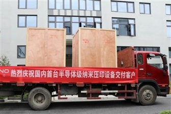
Amid tightening US export controls on EUV lithography systems and related technologies, China's chip equipment sector has made a breakthrough. On August 1, Pulin Technology (Hangzhou) shipped its first domestically developed semiconductor-grade step-and-repeat nanoimprint lithography (NIL) tool, the PL-SR series, to a customer focused on specialized chip manufacturing.
If NIL proves scalable for mass production of advanced chips, it could challenge ASML's dominance in next-gen lithography. The milestone also signals China's progress toward achieving greater autonomy in high-end chip fabrication.
NIL is seen as a next-gen patterning method with the potential to replace or rival EUV and other conventional lithography techniques. It works by pressing nanoscale patterns onto a wafer using a mold, then etching the features into circuit structures. While the concept is simple, achieving semiconductor-level precision and yield demands rigorous control over mold quality, materials, system accuracy, and cleanroom environments — technical hurdles comparable to EUV.
Canon launched its own NIL tool for advanced chipmaking in 2023. The latest version, the FPA-1200NZ2C, was delivered in 2024 to the Texas Institute for Electronics (TIE) in the US.
Pulin's PL-SR series uses inkjet-based step-and-repeat NIL technology designed for sub-10nm nodes and is directly benchmarked against Canon's flagship system. It incorporates proprietary modules for mold profile control, inkjet resist dispensing, precise alignment, and residual layer control. The company claims advances in key metrics, including imprint aspect ratios, resist thickness uniformity, and material compatibility.
The PL-SR system has completed initial process validation for use in memory, silicon photonics, advanced packaging, and microdisplay applications. Its step-and-repeat function supports 12-inch wafer stitching, making it viable for future high-volume deployment.
Precision alignment remains the core hurdle Achieving sub-nanometer alignment accuracy remains a major challenge in chip manufacturing. Pulin's PL-SR addresses this through full-stack co-optimization of hardware, materials, and software, achieving average residual layer thickness under 10nm with less than 2nm variation.
Pulin aims to push alignment precision below 10nm and ultimately approach the 1nm range, bringing NIL into the same technical and economic territory as EUV systems.
The company stressed that tackling these challenges requires collective effort. It plans to strengthen partnerships with local research institutes and precision equipment firms to establish a self-reliant domestic supply chain for advanced chipmaking tools.
The shipment of the PL-SR marks the first commercial deployment of a China-developed step-and-repeat NIL system. Industry insiders see it as a significant shift from lab prototype to practical manufacturing tool.
Founded in 2017, Pulin has focused on core R&D and holds over 50 invention patents. Its NIL platform spans equipment, materials, and processing, placing it among the few globally with end-to-end capabilities in this space.
Over 300 Chinese players engaged in advanced lithography R&D China's progress in lithography was on display at the 2025 Advanced Lithography Technology Symposium in Suzhou, which drew participation from more than 300 domestic research institutes and companies. The event focused on next-gen lithography processes, equipment R&D, and materials innovation, reflecting China's broader push for self-sufficiency in chipmaking.
Key academic participants included Huazhong University of Science and Technology, Fudan University, and the Chinese Academy of Sciences. Domestic equipment makers like AMIES Technology and Hefei Haoyu Xinguang Technology presented progress in EUV laser components, multi-beam lithography, and packaging tools.
With global semiconductor supply chains growing more fragmented, China's push to build indigenous exposure and processing equipment could reshape the global competitive landscape.
Although China still trails global leaders like ASML and Canon in lithography, companies like Pulin are emerging as credible challengers with the potential to replace foreign tools in select applications.
China ships first NIL lithography tool as 300-plus firms mobilize to rival EUV tech
Amid tightening US export controls on EUV lithography systems and related technologies, China's chip equipment sector has made a breakthrough. On August 1, Pulin Technology (Hangzhou) shipped its first domestically developed semiconductor-grade step-and-repeat nanoimprint lithography (NIL) tool...
www.digitimes.com