You are currently viewing SemiWiki as a guest which gives you limited access to the site. To view blog comments and experience other SemiWiki features you must be a registered member. Registration is fast, simple, and absolutely free so please, join our community today!
The worldwide TSMC 2025 Technology Symposium recently kicked off with the first event in Santa Clara, California. These events typically focus on TSMC’s process technology and vast ecosystem. These items were certainly a focus for this year’s event as well. But there is now an additional item that shares the spotlight – packaging technology. Thanks to the increase in heterogeneous integration driven in large part by AI, the ability to integrate multiple dies in sophisticated packages has become another primary driver for innovation. So, let’s look at what was shared at the pre briefing by Dr. Kevin Zhang and how TSMC brings packaging center stage with silicon.
A Growing Palette of Options
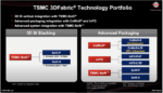
TSMC has taken advanced packaging well beyond the 2.5D interposer approach that is now quite familiar. The diagram above was provided by TSMC to illustrate the elements that comprise the TSMC 3DFabric® technology portfolio. According to TSMC, transistor technology and advanced packaging integration technology go hand-in-hand to provide its customers with a complete product-level solution.
On the left are the options for stacking or die-level/wafer-level integration. SoIC-P ( below) uses microbump technology to deliver down to a 16um pitch. Using bumpless technology (SoIC-X), you can achieve a few micron pitch. TSMC started with 9um and is now in production at 6um with more improvements to come, creating a monolithic-like integration density.
For 2.5/3D integration, there are many options available. Chip on Wafer on Substrate (CoWoS) technology supports both the familiar silicon interposer as well as CoWoS-L, which uses an organic interposer with a local silicon bridge for high-density interconnect. CoWos-R provides a pure organic interposer.
Integrated Fan-Out (InFO) technology began in 2016 for mobile applications. The platform has been expanded to support automotive applications as well.
There is also the newer System-on-Wafer (TSMC-SoW™) packaging. This technology broadens the integration scale to the wafer level. There is a chip-first approach (SoW-P), where the chip is put on the wafer and then an integrated RDL is built to bring the dies together. Or, there is a chip-last approach (SoW-X), where you first build the interposer at the wafer level and then add the chips across the wafer. This last approach can produce a design that is 40X larger than the standard reticle size.
High-performance computing for AI is clearly a major driver for advanced packaging technology. The first diagram below provided by TSMC, illustrates a typical AI accelerator application today that integrates a monolithic SoC with HBM memory stacks through a silicon interposer. Some major improvements that are coming for this type of architecture as shown on the next diagram.
The monolithic SoC is now replaced with a 3D stack of chips to address high-density compute requirements. HBM memory stacks are integrated with an RDL interposer. Integrated silicon photonics will also be part of the design to improve communication bandwidth and power. Integrated voltage regulators will also help to optimize power for this type of application.
Regarding power optimization, future AI accelerators can require thousands of watts of power, creating a huge challenge in terms of power delivery into the package. Integrated voltage regulators will help to tame this class of problem. TSMC has developed a high-density inductor which is a key component required to develop this class of regulator. So, a monolithic PMIC plus this Inductor can provide a 5X power delivery density (vs. PCB level).
There are many exciting new technologies on the horizon which will require all the packaging innovation discussed here. Augmented reality glasses is one example of a new product that will require everything discussed. A device like this will require, among other things, an ultra-low power processor, a high resolution camera for AR sensing, eNVM for code storage, a large main processor for spatial computing, a near-eye display engine, WiFi/Bluethooth for low latency RF, and a digital intensive PMIC for low power charging. This kind of product will set a new bar for complexity and efficiency.
While autonomous vehicles get a lot of attention, the demands of humanoid robots were also discussed. TSMC provided the graphic below to illustrate the significant amount of advanced silicon required. And the ability to integrate all of this into dense, power efficient packages is critical as well.
To Learn More
It was clear at the TSMC Technology Symposium that advanced processing and advanced packaging will need to work as one going forward to achieve the type of product innovation on the horizon. TSMC has clearly taken this challenge and is developing unified offerings to address the coming requirements.
At the pre-conference briefing, Dr. Kevin Zhang gave quite a few of us media types an overview of what will be highlighted at the 2025 TSMC Technical Symposium here in Silicon Valley. Since most of the semiconductor media are not local this was a very nice thing to do. I will be at the conference and will write more tomorrow after the event. TSMC was also kind enough to share Kevin’s slides with us.
The important thing to note is that TSMC is VERY customer driven so this presentation is based on interactions with the largest semiconductor manufacturing customer base the industry has ever seen, absolutely.
As you can imagine, AI is driving the semiconductor industry now not unlike what smartphones did for the last two decades. The difference being that AI consumes leading edge silicon at an alarming rate which is a good thing for the semiconductor industry. While AI is very performance centric, it must also be power sensitive. This puts TSMC in a very strong position from all of those years of manufacturing mobile SOCs for smartphones and other battery operated devices.
Kevin started with the AI revolution and how AI will be infused into most every electronic device from the cloud to the edge and will enable many new applications. Personally, I think AI will transform the world in a similar fashion as smartphones have but on a much grander scale.
Not long ago the mention of the semiconductor industry hitting $1T seemed like a dream. It is one thing for industry observers like myself to say it but it is quite another when TSMC does. There is little doubt in my mind that it will happen based on my observations inside the semiconductor ecosystem.
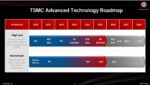
There have been some minor changes to the TSMC roadmap. It has been extended out to 2028 adding N3C and A14. The C is a compressed version meaning the yield learning curve is at a point where the process can be further optimized for density.
A14 will certainly be a big topic of discussion at the event. A14 is TSMC’s second generation of nanosheet transistor which is considered a full node (PPA) versus N2: 10-15% speed improvement at the same power, 25-30% power reduction at the same speed, and 1.2X logic density improvement. The first iteration of 14A does not have backside power delivery. It was the same with N2 which was followed by A16 with Super Power Rail (SPR). SPR for A14 is expected in 2029.
The TSMC 16A specs were updated as well. 16A is the first version of SPR for reduced IR drop and improved logic density. This has the transistor connection on the back. SPR is targeted at AI/HPC designs with improved signal routing and power delivery. A16 is on track for production in the second half of 2026. In comparison to N2P, A16 provides an 8-10% speed improvement at the same power, 15-20% power reduction at the same speed.
From what I have heard TSMC N2 is yielding quite well and is on track for production later this year. The big question is who will be the first customer to ship N2 product? Usually it is Apple but word on the street is the iPhones this year will again be using N3. I already have an N3 iPhone so I will skip this generation if that is the case. If Apple does an N2 based iPhone Max Pro this year then count me in!
TSMC N2P is also on track for production in the second half of 2026. As compared to N3E, N2P offers: 18% speed improvement at the same power, a 36% power reduction at the same speed, and a 1.2x density improvement.
The most interesting thing about N2 is the rapid growth of tape-outs between N5, N3, and N2. It really is astounding. Given that TSMC N3 was an absolute landslide for customer tape-outs I had serious doubts if we would ever see a repeat of that success but here we are. Again, in the past mobile was the driver for early tape-outs but now we have AI/HPC as well.
Finally, as Kevin said, TSMC N3 is the last and best FinFET technology available on such a massive scale with N3, N3E, N3P, N3X, N3A, and now N3C. Yet, N2 tape-outs beat N3 in the first year and the second year even more so. Simply amazing. I guess the question is who is NOT using TSMC N2?
The second part of the presentation was on packaging which will be covered in another blog. After the event I can provide even more details and get a feeling for the vibe at the event from the ecosystem. Exciting times!
UPDATE: TSMC is sharing recordings of the presentations HERE.
In a 2017 ISPD presentation, TSMC Fellow LC Lu outlined critical challenges and innovations in physical design to sustain power, speed, and area scaling trends in semiconductors. As Moore’s Law faces economic hurdles, process-design co-optimization emerges as key to extending it. Lu emphasized application-optimized platforms for mobile, high-performance computing (HPC), automotive, and IoT, balancing area, performance, and power (PPA) with functional safety and ultra-low power needs.
Semiconductor trends highlight slowing primary dimension scaling (metal, gate, fin pitches), making area reduction harder. Innovations like fin depopulation boost cell density by reducing fins from 3-4 in 16nm to 2 in 7nm, easing scaling pressure. This not only increases logic density by up to 3x but also enhances speed-power efficiency: higher-fin cells offer peak speed, while fewer fins excel at same-power speed or same-speed low power. Cell utilization rises from 70% to 80%, aided by power plan optimizations.
Power grid (PG) enhancements are pivotal for logic density. To counter IR drop, PG via counts increase across generations, but shrinking pitches harms routing. Evolving from uniform to dual M1 architectures via top-down or bottom-up co-design allows better cell placement freedom. Power stubs over straps maximize cells under PG, and staggered pins add access points (from 5 to 6), minimizing unused space.
Extreme Ultraviolet (EUV) lithography further densifies routing. Compared to inverse lithography or multiple patterning, EUV single patterning and directed self-assembly (DSA) enable finer pitches (12-16nm half-pitch). Shifting metal:poly pitch from 1:1 to 2:3 provides more metal resources, reducing coupling capacitance and boosting routing tracks, though requiring dual library sets for offsets.
Performance scaling grapples with exponential metal/via resistance growth—up to 3x from 40nm to 5nm—dominating delay (50% BEOL impact at 5nm). Via pillars mitigate this: large drivers, thick upper metals, and pillar structures slash transistor, wire, and via resistance. Automated EDA flows insert electromigration (EM) and performance via pillars across placement, CTS, and routing, reducing BEOL delay impact significantly.
Power scaling leverages ultra-low voltage (ULV) for IoT efficiency, but challenges functionality and variation. Solutions include skew/fine-grained cells, high-stack designs, transmission gates, and multi-bit flops to curb delay degradation. Flop robustness demands high-sigma checks for write paths. Delay variation explodes at low VDD, turning non-Gaussian; new models split distributions into early/late for accurate STA, aligning with Monte Carlo simulations via advanced statistical OCV.
Heterogeneous integration via 3D packaging achieves low-cost, high-performance systems. InFO (Integrated Fan-Out) and CoWoS (Chip-on-Wafer-on-Substrate) outperform traditional SIP/MCM, enabling vertical stacking for better form factors and bandwidth. InFO variants (PoP, Multi-chip) suit small dies (<400mm², <1000 I/Os), while CoWoS handles large HPC integrations (>1000mm², >3000 I/Os). Co-design flows incorporate inter-die DRC/LVS, SI/PI simulations, thermal-aware EM/IR, yielding 12% better thermal dissipation and 5-10% voltage droop reduction in InFO-PoP with IPD.
Machine learning (ML) tackles rising physical design complexity. TSMC’s platform extracts features from APR databases, trains models to predict routing congestion and detours, eliminating biases in traditional EDA heuristics. This enables pre-route optimizations, like accurate ARM A72 clock gating, boosting post-route speed by 40-150MHz with 95% detour prediction accuracy.
In conclusion, these innovations—fin depopulation, EUV, via pillars, ULV modeling, 3D integration, and ML—extend Moore’s Law through EDA-physical design synergy. As nodes shrink, such co-optimizations ensure complex 3D SoCs meet PPA demands, driving future mobile, HPC, and IoT advancements.
At IEDM held in December 2024, TSMC presented: “2nm Platform Technology featuring Energy-efficient Nanosheet Transistors and Interconnects co-optimized with 3DIC for AI, HPC and Mobile SoC Applications,” the authors are:
Geoffrey Yeap, S.S. Lin, H.L. Shang, H.C. Lin, Y.C. Peng, M. Wang, PW Wang, CP Lin, KF Yu, WY Lee, HK Chen, DW Lin, BR Yang, CC Yeh, CT Chan, JM Kuo, C-M Liu, TH Chiu, MC Wen, T.L. Lee, CY Chang, R. Chen, P-H Huang, C.S. Hou, YK Lin, FK Yang, J. Wang, S. Fung, Ryan Chen, C.H. Lee, TL Lee, W. Chang, DY Lee, CY Ting, T. Chang, HC Huang, HJ Lin, C. Tseng, CW Chang, KB Huang, YC Lu, C-H Chen, C.O. Chui, KW Chen, MH Tsai, CC Chen, N. Wu, HT Chiang, XM Chen, SH Sun, JT Tzeng, K. Wang, YC Peng, HJ Liao, T. Chen, YK Cheng, J. Chang, K. Hsieh, A. Cheng, G. Liu, A. Chen, HT Lin, KC Chiang, CW Tsai, H. Wang, W. Sheu, J. Yeh, YM Chen, CK Lin, J. Wu, M. Cao, LS Juang, F. Lai, Y. Ku, S.M. Jang, L.C. Lu- with Jeffrey Yeap presenting the work.
This paper continued TSMC’s trend over the last several years of presenting marketing papers at IEDM instead of technical papers. In fact, this paper took the trend even further, there are no pitches in the paper, no SRAM cell size, and that graphs are all relative performance graphs without real units. Although the paper doesn’t present the kind of technical details that would typically be included in an IEDM paper, it does paint a picture of a process ready for 2025 production and the session was packed.
In this review we will take the few substantive details that are in the paper as well as our own analysis and present how the process compares to competing 2nm class processes.
In terms of the overreaching Power, Performance, and Area (PPA), the paper states that the process delivers a 30% power improvement or 15% performance gain and >1.15x density versus the previous 3nm node. Note: the 3nm paper reference suggests this is in comparison to N3E, not N3.
Power
At the 14nm (Samsung)/16nm (TSMC) node Samsung and TSMC both produced the Apple A9 processors. Measurements by Tom’s hardware found the Samsung version had slightly better power performance compared to TSMC. We believe the A9 was designed for Samsung first so that may simply reflect a design that is more optimized for Samsung that was ported to TSMC, nevertheless, the power was very close between the two. Going forward from 14nm/16nm, to 10nm, 7nm, 5nm, 3nm, and now 2nm Samsung and TSMC have both provided relative power improvement for each node versus the previous node.
We have been able to compare the Samsung and TSMC at 3 different nodes since the 14/16nm comparison and our extrapolations have been consistent with those values.
At 10nm TSMC provided a larger power reduction than Samsung and maintained that lead until 3nm where Samsung Gate All Around (GAA) provided a large enough improvement to mostly close the gap to TSMC’s 3nm FinFET process in power (GAA versus FinFET is expected to provide a greater power improvement).
TSMC 2nm announced power improvement of 30% versus 3nm is greater than Samsung’s 25% improvement and TSMC once again maintains a lead.
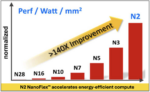
During the presentation of the paper, graphs were shown of power efficiency and performance per watt versus node. The power efficiency graph was in one version of the paper although it is not in the “final” version of the paper published in the proceeding. Thankfully we captured the power efficiency graph because it is very interesting to analyze, see figure 1.
Figure 1. TSMC Power Efficiency.
We took the graph image, pulled it into Excel and created an Excel graph overlaying it with the 28nm bar normalized to 1 and then entering values for the other bars until they matched the graph. If we then build a set of bars starting at 28nm = 1 scaled up based on the TSMC announced node to node power improvements we get a total improvement of less than 9x. Nodes from N28 to N10 match well but from N7 on the bars on the graph show more improvement per node than TSMC has announced. Just the N3 to N2 bars on the graph show a 55% improvements versus the announced 30% improvement.
It isn’t clear what may be driving this difference, but it is a big disconnect. This may be why the graph was removed from the final paper.
Performance
Similar to the power analysis above, at Samsung 14nm/TSMC 16nm the Apple A9 processor had identical performance on the 2 processes. Normalizing both processes to 1 and applying the announced node to node performance improvements from both companies it is possible to compare performance per node. It has also been possible to use an Intel 10SF versus AMD processors on TSMC 7nm process, to add Intel to the analysis and forward calculate based on Intel performance by node announcements.
We have been able to check our extrapolations at 3 nodes for Samsung and TSMC since the 16/14nm nodes as well as Intel at 2 nodes and those checks have confirmed our extrapolations are tracking correctly.
Based on this analysis it is our belief that Intel 18A has the highest performance for a 2nm class process with TSMC in second place and Samsung in third place.
Our performance index values are in the full article available with free registration on the TechInsights platform here.
Area
The third part of PPA is area. We analyze two “area” related factors, one is high density logic cell transistor density and the second is SRAM cell size. TechInsights has done detailed reverse engineering work on TSMC N3E process and we have all the pitches necessary to calculate our standard high density logic cell transistor density. Similarly, we have analyzed Samsung SF3E and SF3. Both TSMC in this paper and Samsung in public statements have provided density improvement values for 2nm. In the case of Intel we have used our own estimated pitches to do a density comparison. For high density logic cells TSMC is well ahead of Samsung and Intel on density, Intel is second, and Samsung is third.
The high density logic cell transistor density is in the full article available with free registration on the TechInsights platform here.
As previously mentioned, the TSMC paper does not include SRAM cell sizes, however there is a graph of SRAM density versus node, see figure 3.
Figure 3. SRAM Array Density Versus Node.
The problem with this is an SRAM array includes not only the SRAM cell but also overhead, for example 7nm has 25.0 Mb/mm2, the SRAM cell size at 7nm was 0.0270um2. If you multiply 25.0Mb by the SRAM cell size, you get 0.675mm2. The difference between 1.000 and 0.675mm2 is the overhead and it isn’t constant from node to node, see table 1.
Yield
Yield is a hot topic these days with lot of reports about Samsung struggling with yield at 3nm and losing customers due to low yield, there have also been some recent reports that Intel’s 18A yield is 10%.
In the paper TSMC reports that a 256Mb SRAM array has >80% average yield and >90% peak yield. These yields at this point in development indicate excellent defect densities. There are other yield components beside those tested in an SRAM array, but these are impressive results.
With respect to Intel’s 10% yield report, we have had two separate credible sources that tell us that simply isn’t true, that yields are much better than that. The other things about a report of 10% yield is how big/what is the die and at what point in development was that yield seen if it is even true. Our belief based on our sources is the 10% reported yield is either wrong or old data.
Wafer price
Another number that has been widely circulated is that TSMC is going to charge $30,000 per wafer for 2nm.
TechInsights produces the world’s leading cost and price models for semiconductors. Prior to 3nm entering production we were projecting <$20,000 per wafer and a few customers contacted us insisting 3nm prices would be $20,000 to $25,000 per wafer. Once 3nm entered production we were able to run our proprietary forensics on TSMC’s financials and determine we were correct, and the volume price was <$20,000/wafer by thousands of dollars.
To go from a price of <$20,000/wafer for 3nm wafers to $30,000/wafer for 2nm wafers is a >1.5x price increase for a 1.15x density improvement, that is a dramatic increase in transistor cost and it raises the question of who would pay that, our price estimates are <$30,000/wafer. There have also been reports that Apple who is typically TSMC’s lead customer for each node may be forgoing initial 2nm use due to price although we have also heard push back on that.
Another element to this discussion is what volumes the pricing is for TSMC’s high volume wafer price is a lot lower than their low volume wafer price, so volume needs to be considered in any discussion. In general, we believe $30,000 is higher than the average to high volume pricing will be.
If TSMC prices 2nm wafers at $30,000/wafer they will create a lot of pressure for customers to switch to Intel and Samsung for 2nm class wafer supplies.
Backside Power Delivery
The TSMC paper does not address backside power delivery but competing 2nm processes will be implementing backside power delivery.
Intel 18A will have backside power delivery – with a 2025 ramp Intel will be the first to implement this technology. In 2026 Samsung SF2P process is due to also implement backside power delivery. Finally, TSMC is not expected to implement backside power delivery on their 2nm process variants at all and will wait until 2027 (recent reports are that this is being pulled in to 2026) to implement it on their A16 process. The A16 backside power delivery is expected to be a direct backside connection that can provide smaller track heights than Intel’s and likely Samsung’s implementation.
Since Intel is the most performance focused of the three companies it makes sense, they are implementing backside power delivery first.
Another interesting thing we are hearing about backside power delivery is that foundry HPC customers want it but mobile customers don’t due to cost.
For multiple nodes we may see nodes with and without backside power delivery and given the effect it has on metal 0 the design rules would likely be different. In addition to this for the highest performance we expect molybdenum to be introduced first for vias and later from critical interconnect. This could lead to nodes splitting between backside power delivery and molybdenum metallization for HPC and no backside power and copper metallization for mobile.
Other
One final interesting item in the paper is the comment about “flat passivation”. Many processes have a top aluminum metal layer and passivation follows the metal contours, if something like hybrid bonding is desired the wafer surface must be flat. Flat passivation is presumably a planarized top layer to enable bonding.
Conclusion
TSMC has disclosed a 2nm process likely to be the densest available 2nm class process. It also appears to be the most power efficient at least when compared to Samsung. In terms of performance, we believe Intel 18A is the leader. The early yield reports appear promising, but the reports of $30,000/wafer pricing do not in our opinion represent acceptable value for the process and may present an opportunity for Intel and Samsung to capture market share . TSMC 2nm should be in production in the second half of this year.
Advantest Corporation, a world-leading supplier of semiconductor test equipment, has been honored with the Excellent Performance Awardat the 2025 Taiwan Semiconductor Manufacturing Company (TSMC) Supply Chain Management Forum. This recognition, presented by one of the semiconductor industry’s most influential companies, marks a major milestone in Advantest’s ongoing efforts to strengthen collaboration with TSMC and extend its impact across the global semiconductor supply chain.
The award was bestowed during TSMC’s annual Supply Chain Management Forum held on November 25, 2025, which brought together key supplier partners from around the world. The forum serves as a platform to celebrate the contributions of companies that have demonstrated exceptional performance in improving efficiencies, supporting production, and contributing to the resilience and sustainability of the semiconductor ecosystem.
For Advantest, this award is particularly meaningful — it is the first time the company has received this honor at TSMC’s forum. Advantest was recognized in the category of Excellent Production Support, reflecting the company’s ability to adapt to rapidly shifting demand, flexibly expand production capacity, and provide critical project support to TSMC’s advanced manufacturing operations.
One of the key reasons Advantest stood out among its peers was its responsiveness to urgent demand. In an era marked by supply chain constraints and explosive growth in semiconductor demand, especially for advanced nodes and high-performance computing chips, Advantest demonstrated a remarkable capacity to scale tooling and manpower efficiently. By doing so, it helped TSMC maintain production momentum and meet customer requirements on time.
The evaluation framework for this year’s awards also placed greater emphasis on construction safety, sustainability, and localization efforts, aligning with broader industry trends toward responsible and resilient supply chains. TSMC’s focus on these areas reflects the increasing importance of sustainable operations and safe working environments in semiconductor production — areas where partners like Advantest have begun to differentiate themselves.
Doug Lefever, Representative Director and Group CEO of Advantest, accepted the award in person at the forum. In his remarks, Lefever expressed deep appreciation for the recognition, stating that Advantest is “thrilled to be recognized by one of our most respected partners.” He reaffirmed the company’s commitment to serving partners throughout the supply chain and to continuing collaboration that enhances both innovation and resilience in the semiconductor industry.
The award was presented by Dr. Cliff Hou, Senior Vice President and Deputy Co-COO of TSMC, underscoring the strategic nature of Advantest’s relationship with the world’s largest contract chip manufacturer. This official acknowledgment from senior leadership highlights the trust and value inherent in the Advantest-TSMC partnership.
Advantest’s recognition at the 2025 Supply Chain Management Forum coincides with a broader period of growth and industry leadership for the company. The firm’s extensive portfolio, which includes SoC and memory testers, handlers, software solutions, system-level test (SLT) equipment, device interfaces, and field service support, positions it as an essential contributor to semiconductor innovation and production excellence. Its products serve critical roles at multiple stages of semiconductor manufacturing, from design verification to final test and quality assurance.
The semiconductor industry continues to experience rapid transformation driven by key trends such as the rise of 5G communications, the Internet of Things (IoT), autonomous vehicles, and artificial intelligence (AI). These technologies demand increasingly sophisticated chip designs and manufacturing capabilities, amplifying the need for robust testing and quality assurance solutions — precisely the areas where Advantest excels.
Bottom line: Receiving the Excellent Performance Award not only reinforces Advantest’s reputation as a trusted supplier to TSMC but also signals broader confidence in its capabilities across the semiconductor ecosystem. As global demand for advanced semiconductors continues to surge, partnerships like the one between Advantest and TSMC will be key to driving innovation, operational excellence, and sustainable supply chain practices in the years ahead.
There was a lot of discussion at IEDM about the coming shift to gate-all-around (GAA) transistor structures. This new device brings many benefits to continue device scaling, both at the monolithic device level as well as for multi-die design. The path to GAA is not simple, there are new material, process and design considerations to tame. TSMC has devoted a substantial amount of effort here. Let’s look at some of the details disclosed when TSMC unveils the world’s most advanced logic technology at IEDM.
About the Presenter
Dr. Geoffrey Yeap
Dr. Geoffrey Yeap presented 2nm Platform Technology featuring Energy-efficient Nanosheet Transistors and Interconnects co-optimized with 3DIC for AI, HPC and Mobile SoC Applications on Monday at IEDM. He is Vice President, TSMC R&D Advanced Technology. Geoffrey has been at TSMC for almost nine years and has also led advanced work at Qualcomm, Motorola Mobility, AMD, and the University of Texas System Center for Supercomputing.
Geoffrey explained that the work he was presenting spanned four years and involved many staff members in TSMC’s Global R&D Center.
Presentation Overview
According to the IEDM press kit, this late news paper presents the world’s most advanced logic technology. As the title says, the work is focused on a leading edge 2nm CMOS platform technology (N2) that has been developed and engineered for energy-efficient compute in AI, mobile and HPC applications. Geoffrey explained that since the generative AI break-through in Q1’23, AI together with 5G-advanced mobile and HPC have created a huge appetite in the semiconductor industry for best-in-class energy-efficient logic technology and this work responds to that need.
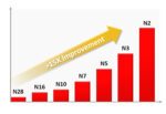
Geoffrey described the state-of-art TSMC N2 technology and its successful transition into NS platform technology with acceleration of >140x energy-efficient compute from 28nm to N2, as depicted in the graphic at the top of this post. The N2 logic technology features energy-efficient gate-all-around nanosheet transistors, middle-of-line and backend-of-line interconnects with the densest SRAM macro of ~38Mb/mm2. N2 delivers a full node benefit from the previous 3nm node in offering 15% speed gain or 30% power reduction with >1.15x chip density increase.
The N2 platform technology is equipped with new copper scalable RDL interconnect, flat passivation and TSVs. It co-optimizes holistically with TSMC’s 3DFabric™ technology enabling system integration/scaling for the target AI/mobile/HPC product designs.
Geoffrey reported that N2 has successfully met wafer-level reliability requirements and passed 1,000 hours of HTOL qualification with high yielding 256Mb HC/HD SRAM, and logic test chip (>3B gates) consisting of CPU/GPU/ SoC blocks. N2 is currently in risk production. N2 platform technology is scheduled for mass production in the second half of 2025. N2P, a 5% speed enhanced version of N2 with full GDS compatibility, is targeted to complete qualification in 2025 and go to mass production in 2026.
Some More Details
From a platform perspective, Geoffrey provided some details about the N2 NanoFlex™ technology architecture. System technology co-optimization (STCO) was utilized with smart scaling features rather than brute-force design rule scaling which can drastically increase process cost and inadvertently causes critical yield issues. Extensive STCO coupled with smart scaling of major design rules (e.g., gate, nanosheet, MoL, Cu RDL, passivation, TSVs) was performed in optimizing the technology to achieve the target PPA.
He pointed out that co-optimization with 3DFabric SoIC 3D-stacking and advanced packaging technology (INFO/CoWoS variants) was done, thereby accelerating system integration/scaling for AI/mobile/HPC product designs. N2 NanoFlex standard cell innovation offers not only nanosheet width modulation but also a much-desired design flexibility of a multi-cell architecture.
This capability delivers N2 short cell libraries for area and power efficiency. He explained that selective use of tall cell library elements lifts the frequency to meet design targets. With six Vt offerings spanning 200mV, N2 provides unprecedented design flexibility to satisfy a wide spectrum of energy-efficient compute applications at the best logic density. The figure below illustrates some of the benefits of this approach for an Arm-based design.
N2 NanoFlex HD cell benefits
Geoffrey explained that N2 nanosheet technology exhibits substantially better performance/Watt than FinFET at the low Vdd range of 0.5V- 0.6V. Emphasis is placed on low Vdd performance/Watt uplift through process and device continuous improvements resulting in a 20% speed gain and 75% lower stand-by power at 0.5V operation. N2 NanoFlex coupled with multi-Vt provides unprecedented design flexibility to satisfy a wide spectrum of energy-efficient compute applications at the most competitive logic density.
Geoffrey went into more details on the SRAM, logic test chip and qualification and reliability. This was an impressive presentation. The N2 technology platform brings a lot of new capability to the table for future innovation. And that’s some of the details about how TSMC unveils the world’s most advanced logic technology at IEDM.
The main program for the 70th IEDM opened on Monday morning in San Francisco with an excellent keynote from Dr. Yuh-Jier Mii, Executive Vice President and Co-Chief Operating Officer at TSMC. Dr. Mii joined TSMC in 1994. Since then, he has contributed to the development and manufacturing of advanced CMOS technologies in both fab operations and R&D. In 2022, he received the IEEE Frederik Philips Award recognizing his outstanding accomplishments in the management of research and development. He holds 34 patents globally, including 25 US patents, and holds a B.S. in electrical engineering from National Taiwan University, as well as an M.S. and Ph.D. in Electrical Engineering from the University of California, Los Angeles (UCLA). He treated the audience to a broad view of technology innovation in his keynote. Let’s look at how IEDM opens with a big picture keynote from TSMC’s Yuh-Jier Mii.
About IEDM
To begin, that wasn’t a typo above. The 70th annual IEEE International Electron Devices Meeting (IEDM) just concluded. This incredibly long-lived conference began tracking technology innovation in the vacuum tube era. For seven decades the event has tracked semiconductor and electronic device technology, design, manufacturing, physics, and modeling. This year’s event had a record high number of submissions at 763 and a record number of accepted papers at 274.
The figure below summarizes the growth of this premier conference over the years.
2024 IEDM paper statistics
About the Keynote
Dr. Yuh-Jier Mii
Dr. Mii began his keynote with a short but compelling video that provided an overview of some of the innovations that have occurred in the semiconductor industry in general, and some of the advances contributed by TSMC in particular. All of this is driving the development of a trillion-transistor system in the near future. These trends are summarized in the graphic at the top of this post.
Dr. Mii touched on five key areas in his talk. I will provide a summary of his remarks. He began with a semiconductor industry & market outlook (I). AI is poised to play a key role in the industry’s growth as we move toward one trillion dollars in revenue by 2030. He projected that high-performance computing will contribute 40% of this number, mobile 30%, automotive 15%, and IoT 10%. He discussed the how ubiquitous AI technology is becoming across many products and markets. Generative AI and large language models are contributing to this growth and the complexity of the models for these new applications and the associated training required present substantial new challenges.
He pointed out that these new applications will require gigawatts of power within a few years. Reducing power consumption will be critical to allow these applications to flourish and new device technology and architectural advances will be needed.
Next, Dr. Mii discussed advanced logic technologies (II). He described the industry’s move from planar devices to FinFETs and most recently nanosheet technology for gate-all-around devices at 2nm. Patterning also advanced from immersion lithography to EUV and multi-patterning EUV. Design technology co-optimization, or DTCO has also helped to bring technology to new levels. For example, backside power delivery has helped to reduce power and increase density.
Regarding logic technology frontiers (III), Dr. Mii discussed the evolution from FinFET to nanosheet FET to vertically stacked complimentary or CFET architectures. He explained that the CFET approach holds great promise to allow continued Moore’s Law scaling with its 1.5 – 2X density improvement when compared to nanosheet devices. He described the work going on at TSMC to make CFETs a reality. At this year’s IEDM, TSMC is presenting the first and smallest CFET inverter at a 48nm pitch.
Dr. Mii explained that beyond CFET, the ongoing quest for higher performance and more energy-efficient logic technologies necessitates an accelerated search for channel materials that go beyond those based on silicon. He explained that carbon nanotubes (CNTs) and transition metal dichalcogenides (TMDs) have garnered significant interest due to both their physical and electronic properties. In the area of interconnects, he discussed a new 2D material that is being explored as a superior alternative to copper. This material shows lower thin film resistivity than copper at reduced thicknesses, helping to mitigate line resistance increases in scaled geometries and enhance overall performance.
Dr. Mii then moved to a discussion of system integration technologies (IV). While pushing 2D technology scaling to enable better transistors and higher packing density in monolithically integrated SoCs is important, so are innovations beyond the chip level to extend integration into the heterogenous domain.
He explained that advanced silicon stacking and packaging technologies, including SoIC, InFO, and CoWoS® continue to aggressively scale down the chip-to-chip interconnect pitch, offering the potential to improve 3D interconnect density by another six orders of magnitude. These trends are summarized in the figure below.
Advanced silicon stacking and packaging technologies
Dr. Mii discussed an emerging System-on-Wafer (SoW) technology, where all the chiplets and HBM memories for an entire system can be integrated directly on a 12-inch wafer. He explained that this approach can deliver an additional 40X compute improvement when compared to the most advanced data center AI accelerator today. Optical interconnect was also discussed, which can provide 20X more power efficiency than copper interconnect. Vertical stacking of logic and optical transceivers will help deliver these improvements. He explained that today the laser light source is outside the chip, but efforts are underway to integrate the laser on chip as well.
Dr. Mii concluded with a discussion of specialty technologies (V). Many of the items discussed here are high frequency or analog in nature to accommodate the interface between the digital and analog (real) world. He discussed innovations spanning N16 to N4 to accommodate the increased demands of new standards for WiFi.
Advances in embedded non-volatile RAM were also discussed in this part of the keynote. The benefits and challenges of both MRAM and RRAM were covered. CMOS image sensors were also discussed. This is a critical technology for automotive applications. As pixel size decreases, new approaches are needed to maintain sensitivity and dynamic range. Dr. Mii described work to separate the photo diode from the pixel device and re-integrate them using 3D wafer-to-wafer stacking.
Summary
Dr. Mii concluded by observing that semiconductor innovations, encompassing advances in device technology, system-level scaling, and customer-specific design ecosystems will remain pivotal in driving rapid technological progress in the era of AI. He pointed out that TSMC is actively exploring a new array of innovations for future generations of technology, system integration platforms, and design ecosystems. These efforts will be crucial in meeting the increasing societal demands for energy-efficient, data-intensive computing in the coming decades. He invited the audience to join in this important collaboration. And that’s how IEDM opens with a big picture keynote from TSMC’s Yuh-Jier Mii.
The TSMC Open Innovation Platform (OIP) Ecosystem Forum has become the industry benchmark when it comes to showcasing industry-wide collaboration. The extreme design, integration and packaging demands presented by multi-die, chiplet-based design have raised the bar in terms of required collaboration across the entire supply chain. World-class development and collaboration were on display at the recent event, which was held in Santa Clara on September 25, 2024. A critical technology required for success is enabling IP, in particular for sensing and power management. Analog Bits showcased substantial capabilities here. Let’s examine some of the work presented to see how Analog Bits builds a road to the future at TSMC OIP.
IP Development Progress
Analog Bits discussed some of the unique challenges advanced chip and multi-die design presents. Multi-domain sensing was discussed, along with the additional challenge of non-uniform thermal distributions. Real-time monitoring is another requirement. If the face of all this, calibration complexity, voltage supply noise, and crosstalk must all be dealt with as well.
Analog Bits portfolio of on-die sensing IP was presented, including:
PVT Sensors – integrated and pinless
Power on reset and over current detection macros
Power supply detectors that include:
Fast detecting glitch
Synchronized droop detection with filtering and differential sensing
The benefits of a comprehensive on-die sensing IP portfolio were also discussed. At the top of the list is improved power efficiency. A good approach here also prevents overheating and minimizes thermal stress. The overall benefits of enhanced reliability and improved yield also come into play.
Power management is also a key benefit. Things like voltage scalability, voltage spike, and droop protection are examples. Better integration that results in space savings is an added benefit.
Analog Bits presented a significant amount of silicon data based on a TSMC N3P test chip. The graphic at the stop of this post is an overview of what’s on this chip. There were many impressive results to show. Here is a list of some of them:
Temperature linearity and precision for the High-Accuracy Thermometer
Linearity and precision for the high-accuracy Voltage Sensor
Measured trigger voltage vs. threshold and untrimmed threshold accuracy for the Droop Detector
An overview of Low-Dropout (LDO) regulator development
Regarding the LDO, here is a summary of the program:
First LDO modules proven in silicon
Latest N3 test-chip taped out Q2 2024
Packaging and initial bring up Q1 2025
Automotive planned for mid-2025
Here is an example of the data presented. The plot is showing Voltage Sensor accuracy with the following parameters: VDDA: 1.2V, VDD: 0.75V, Corner: TT.
Voltage Sensor Accuracy
IP Collaboration Progress
OIP is all about ecosystem collaboration, so Analog Bits teamed with Arm to present an impressive presentation entitled, Optimized Power Management of Arm CPU Cores with Integrated Analog Bits Power Management and Clocking IP’s. The presenters were Lisa Minwell, Director of Technology Management at Arm and Alan Rogers, President at Analog Bits.
The once-in-a-generation transformation occurring in digital infrastructure was discussed. Complexity increases in data center SoC’s, coupled with AI deployment has made energy efficiency a central issue. It was pointed out that advanced chip and chiplet-based designs in 3nm and 2nm are integrating many Arm Neoverse cores.
The need for managing power to these cores on a granular level is getting increasingly important. The traditional methods of using off-chip LDO and power sensors no longer scales. A new approach is needed.
The work Analog Bits and Arm have done on several integrated power management and clocking IPs was presented. Arm customers can readily use these solutions in N3P and soon in N2P. LDO regulator IPs were also discussed to efficiently manage the large absolute and dynamic current supplies to Arm CPU cores.
A case study of how CPU cores seamlessly integrate with Analog Bits LDO and Power Glitch Detector IPs, along with integrated clocking capabilities was also presented. The implications of this work is substantial for advanced data center applications.
To Learn More
I have presented some of the highlights of Analog Bits presence at TSMC OIP. There is a lot more to the story, and you find out more about Analog Bits industry impact on SemiWiki here. You can also check out the company’s website here. And that’s how Analog Bits builds a road to the future at TSMC OIP.
At the 2024 TSMC OIP Ecosystem Forum, one of the technical talks by TSMC focused on maximizing 3DIC design productivity and rightfully so. With rapid advancements in semiconductor technology, 3DICs have become the next frontier in improving chip performance, energy efficiency, and density. TSMC’s focus on streamlining the design process for these cutting-edge solutions has been critical, and 3DBlox is central to this mission. 3DBlox is an innovative framework inclusive of a standardized design language, introduced by TSMC aimed at addressing the complexities of 3D integrated circuit (3DIC) design. The following is a synthesis of that talk, delivered by Jim Chang, Deputy Director at TSMC for the 3DIC Methodology Group.
Progress from 2022 to 2023: Laying the Foundations for 3DBlox
In 2022, TSMC began exploring how to represent their 3DFabric offerings, particularly CoWoS (Chip-on-Wafer-on-Substrate) and INFO (Integrated Fan-Out), which are critical technologies for 3DIC. CoWoS integrates chips using a silicon interposer, while INFO uses RDL (Redistribution Layer) interposers. TSMC combined these approaches to create CoWoS-R, replacing the silicon interposer with RDL technology, and CoWoS-L, which integrates local silicon interconnects.
With these building blocks in place, TSMC realized that they needed a systematic way to represent their increasingly complex technology offerings. This led to the creation of 3DBlox, which provided a standard structure for representing all possible configurations of TSMC’s 3DFabric technologies. By focusing on three key elements—chiplets, chiplet interfaces, and the connections among interfaces—TSMC was able to efficiently model a wide range of 3DIC configurations.
By 2023, TSMC had honed in on chiplet reuse and design feasibility, introducing a top-down methodology for early design exploration. This methodology allowed TSMC and its customers to conduct early electrical and thermal analysis, even before having all the design details. Through a system that allowed for chiplets to be mirrored, rotated, or flipped while maintaining a master list of chiplet information, TSMC developed a streamlined approach for design rule checking across multiple chiplets.
Innovations in 2024: Conquering Complexity with 3DBlox
By 2024, TSMC faced the growing complexity of 3DIC systems and devised new strategies to address it. The key innovation was breaking down the 3D design challenge into more manageable 2D problems, focusing on the Bus, TSVs (Through-Silicon Vias), and PG (Power/Ground) structures. These elements, once positioned during the 3D floorplanning stage, were transformed into two-dimensional issues, leveraging established 2D design solutions to simplify the overall process.
Key Technology Developments in 2024
TSMC’s focus on maximizing 3DIC design productivity in 2024 revolved around five major areas of development: design planning, implementation, analysis, physical verification, and substrate routing.
Design Planning: Managing Electrical and Physical Constraints
In 3DIC systems, placing the Bus, TSVs, and PG structures requires careful attention to both electrical and physical constraints, especially Electromigration and IR (EMIR) constraints. Power delivery across dies must be precise, with the PG structure sustaining the necessary power while conserving physical resources for other design elements.
One of TSMC’s key innovations was converting individual TSV entities into density values, allowing them to be modeled numerically. By using AI-driven engines like Cadence Cerebrus Intelligent Chip Explorer and Synopsys DSO.ai, TSMC was able to explore the solution space and backward-map the best solutions for bus, TSV, and PG structures. This method allowed designers to choose the best tradeoffs for their specific designs.
Additionally, chip-package co-design was emphasized in 2024. TSMC collaborated with key customers to address the challenges of coordinating between the chip and package teams, which previously operated independently. By utilizing 3DBlox’s common object format and common constraints, teams could collaborate more efficiently, settling design constraints earlier in the process, even before Tech files were available.
Implementation: Enhancing Reuse and Hierarchical Design
As customers pushed for increased chiplet reuse, TSMC developed hierarchical solutions within the 3DBlox language to support growing 3DIC designs. With the increasing number of alignment marks required to align multiple chiplets, TSMC worked closely with EDA partners to identify the four primary types of alignment markers and automate their insertion in the place-and-route flow.
Analysis: Addressing Multi-Physics Interactions
Multi-physics interactions, particularly related to thermal issues, have become more prominent in 3DIC design. TSMC recognized that thermal issues are more pronounced in 3DIC than in traditional 2D designs due to stronger coupling effects between different physical engines. To address this, TSMC developed a common database that allows different engines to interact and converge based on pre-defined criteria, enabling efficient exploration of the design space.
One of the critical analysis tools introduced in 2024 was warpage analysis, crucial as the size of 3DIC fabric grows. TSMC developed the Mech Tech file, defining the necessary information for industry partners to facilitate stress simulation, addressing a gap in warpage solutions within the semiconductor industry.
Physical Verification: Ensuring Integrity in 3DIC Designs
TSMC tackled the antenna effect, a manufacturing issue where metal may accumulate plasma charges that can penetrate gate oxides via TSVs and bumps. By collaborating with EDA partners, TSMC created a design rule checking (DRC) deck that models and captures the antenna effect, ensuring it can be accounted for during the design process.
In 2024, TSMC also introduced enhancements in layout vs. schematic (LVS) verification for 3DIC systems. Previously, LVS decks assumed a one-top-die, one-bottom-die configuration. However, 3DBlox’s new automated generation tools allow for any configuration to be accurately verified, supporting more complex multi-die designs.
Substrate Routing: Tackling the Growing Complexity
As 3DIC integration grows in scale, so does the complexity of substrate routing. Substrate design has traditionally been a manual process. The growing size of substrates, combined with the intricate requirements of modern 3DIC designs, necessitated new innovations in this space.
TSMC’s work on Interposer Substrate Tech file formats began three years ago, and by 2024, they were able to model highly complex structures, such as the inclusion of tear drops in the model. This advancement offers a more accurate and detailed representation of substrates, crucial for the larger and more intricate designs emerging in the 3DIC space. TSMC worked with their OSAT partners through the 3DFabric Alliance to support this format.
Summary: 3DBlox – Paving the Way for 3DIC Innovation
TSMC’s 3DBlox framework has proven to be a crucial step in managing the complexity and scale of 3DIC design. From early exploration and design feasibility in 2023 to breakthroughs in 2024 across design planning, implementation, analysis, physical verification, and substrate routing, TSMC’s innovations are paving the way for more efficient and scalable 3DIC solutions. As the industry moves toward even more advanced 3D integration, the 3DBlox committee announced plans to make the 3DBlox standard publicly available through IEEE. 3DBlox will continue to play a vital role in enabling designers to meet the increasing demands of semiconductor technology for years to come.
Synopsys made significant announcements during the recent TSMC OIP Ecosystem Forum, showcasing a range of cutting-edge solutions designed to address the growing complexities in semiconductor design. With a strong emphasis on enabling next-generation chip architectures, Synopsys introduced both new technologies and key updates to existing solutions in collaboration with TSMC.
At the heart of this collaboration is the goal of accelerating the development of trillion-transistor chips, which are necessary to support the computational demands of Artificial Intelligence (AI) and high-performance computing (HPC) applications. As these systems continue to grow in complexity, Synopsys and TSMC are collaborating to leverage AI to streamline the design process and ensure power efficiency, scalability, and system reliability. What caught my interest and attention was the focus multi-die, 3D Integrated Circuits (3DICs), and multi-physics design analysis are receiving in this collaboration. Before we dive into that, below is a roundup of the key announcements.
Roundup of the Key Announcements from Synopsys
Synopsys aims to enable the design of more complex, efficient, and scalable multi-die packages that can meet the evolving demands of AI, HPC, and other advanced computing applications.
Synopsys.ai Suite Optimized for TSMC N2 Process Technology: This was a key update, as Synopsys’ AI-driven EDA suite was already known for its ability to improve Quality of Results (QoR). The latest optimization focuses on the N2 process, helping designers move more swiftly to next-generation nodes while enhancing chip performance and power efficiency.
Backside Power Delivery in TSMC A16 Process: A new innovation that stood out was the backside power delivery system, which promises more efficient power routing and reduced energy consumption. This method helps manage the demands of trillion-transistor architectures by optimizing signal integrity and chip density.
Synopsys IP Solutions for 3DFabric Technologies: Updates were made to Synopsys’ UCIe and HBM4 IP solutions, which are crucial for TSMC’s 3DFabric technologies, including CoWoS (Chip on Wafer on Substrate) and SoIC (System on Integrated Chips). These updates further improve bandwidth and energy efficiency in multi-die designs.
3DIC Compiler, 3DSO.ai and Multi-Physics Flow: One of the more notable announcements involved the enhancement of Synopsys’ 3DIC Compiler platform and 3DSO.ai to address the complexities of multi-die designs and offer AI-driven multi-physics analysis during the design process, helping to streamline system-level integration.
TSMC Cloud Certification for Accelerated Design: To further accelerate the design process, Synopsys and TSMC have also enabled Synopsys EDA tools on the cloud, certified through TSMC’s Cloud Certification. This provides mutual customers with cloud-ready EDA tools that not only deliver accurate QoR but also seamlessly integrate with TSMC’s advanced process technologies.
The Importance of Multi-Die, 3DIC, and Multi-Physics Design
As semiconductor technology pushes beyond the traditional limits of Moore’s Law, multi-die designs and 3DICs have become essential for enhancing performance and density. These technologies allow for multiple dies, each with its own specialized function, to be stacked or placed side-by-side within a single package. However, the integration of these dies—especially when combining electronic ICs with photonic ICs—introduces significant design challenges.
One of the most pressing issues in multi-die design is thermal management. As multiple heat-generating dies are placed in close proximity, the risk of overheating increases, which can degrade performance and shorten the lifespan of the chip. Additionally, electromagnetic interference (EMI), signal integrity, and power distribution present further challenges that designers must account for during early-stage development.
This is where multi-physics analysis plays a critical role. Multi-physics analysis is the process of evaluating how different physical phenomena—such as heat dissipation, mechanical stress, and electrical signals—interact with one another within a chip package. Without an understanding of these interactions, it becomes nearly impossible to design reliable and efficient multi-die systems.
Synopsys Solutions for Multi-Die and 3DIC Challenges
Synopsys is at the forefront of addressing these challenges through its AI-powered solutions, many of which were updated or introduced during the TSMC OIP Ecosystem Forum. These tools are specifically designed to address the complexity of multi-die designs and 3DICs, where early-stage analysis and optimization are crucial for success.
AI-Driven EDA with Synopsys.ai
One of the most significant updates came from Synopsys.ai, which is now optimized for TSMC’s N2 process technology. This suite allows designers to leverage AI to improve design efficiency and reduce the time needed to move designs to production. By incorporating AI into the design process, Synopsys.ai helps engineers navigate the vast array of potential design configurations, ensuring that the most optimal solutions are chosen for performance, power efficiency, and thermal management.
“Synopsys’ certified Custom Compiler and PrimeSim solutions provide the performance and productivity gains that enable our designers to meet the silicon demands of high-performance analog design on the TSMC N2 process,” said Ching San Wu, Corporate VP at MediaTek in Synopsys’ news release. “Expanding our collaboration with Synopsys makes it possible for us to leverage the full potential of their AI-driven flow to accelerate our design migration and optimization efforts, improving the process required for delivering our industry-leading SoCs to multiple verticals.”
3DIC Compiler and 3DSO.ai for Multi-Die Systems
These tools enable designers to conduct multi-physics analysis early in the design process, which is essential for optimizing thermal and power management, signal integrity, and mechanical stability in multi-die systems. By identifying potential issues—such as hotspots or signal degradation—early in the process, designers can make informed adjustments before reaching the later stages of development, thus avoiding costly redesigns.
3DSO.ai leverages AI to analyze complex multi-die configurations, allowing engineers to test a wide range of potential scenarios in a fraction of the time it would take using traditional methods. This capability is critical as designs become more complex, with tens of thousands of possible combinations for how dies are stacked, interconnected, and cooled.
TSMC-certified Synopsys 3DIC Compiler’s compatibility with TSMC’s SoIC and CoWoS technologies further solidify its position as a leading platform for multi-die designs. This ensures seamless collaboration across design architecture and planning, design implementation, and signoff teams, enabling efficient 3DIC development for cutting-edge applications.
These technologies are critical for enabling the heterogeneous integration of dies in 3DIC systems, which helps overcome traditional scaling challenges such as thermal management and signal integrity.
As a demonstration vehicle, Synopsys achieved a successful tapeout recently, of a test chip featuring a multi-die design using TSMC’s CoWoS advanced packaging technology. This test chip leveraged TSMC’s 3DFabric technology and Synopsys’ multi-die solutions, including silicon-proven UCIe IP, 3DIC Compiler unified exploration-to-signoff platform, and the 3DSO.ai AI-driven optimization solution. The Figure below showcases the level of system analysis and optimization enabled by Synopsys 3DSO.ai. The test chip demonstrated unmatched performance reliability.
Figure: Synopsys 3DSO.ai AI-enabled system analysis and optimization
Optimizing Power Delivery with Backside Power Innovations
The new backside power delivery capability, introduced through TSMC’s A16 process, represents a critical leap forward in ensuring power integrity in multi-die systems. By routing power through the backside of the chip, more space is made available on the front for signal routing and transistor placement. This helps reduce energy consumption while also enhancing signal integrity, ensuring that trillion-transistor designs can operate efficiently and reliably.
Summary
The announcements made by Synopsys at the TSMC OIP Ecosystem Forum underscore the growing importance of multi-die architectures, 3DIC systems, and multi-physics analysis in semiconductor design. With new AI-driven tools and key updates to existing solutions, Synopsys is helping engineers overcome the complex challenges posed by trillion-transistor designs and multi-die integration.
By leveraging Synopsys’ advanced EDA tools, platforms and IP, engineers can now address critical issues—like thermal management, signal integrity, and power distribution—at the earliest stages of the design process. This proactive approach not only improves design efficiency but also ensures that the final product meets the stringent performance requirements of AI, HPC, and other next-generation applications.
You can read the Synopsys announcement in its entirety here, and more details on the test chip tapeout here.