EUV lithography is widely perceived to be the obvious choice to replace DUV lithography due to the shorter wavelength(s) used. However, there’s a devil in the details, or a catch if you will.
Electrons have the last word
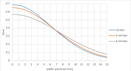
The resist exposure is completed by the release of electrons following the absorption of the EUV photon. Photoelectrons initially released by EUV absorption are expected to be ~ 80 eV, and release energy by further ionization, producing secondary electrons [1]. The photoelectrons and secondary electrons can lose energy by plasmon generation as well [2]. Electrons with energies as low as 1.2 eV can still expose resists [3]. Dissociative electron attachment (DEA) can also occur at very low energies [4]. Consequently, the image is affected by the “blur” resulting from the spread of these electrons. An example is shown below in Figure 1. Even a few nm blur or a few nm blur difference can degrade the sub-20 nm image’s sensitivity to dose variations.
Figure 1. Secondary electron blur is modeled as a Gaussian function involved with the original non-blurred image, fitted with a Gaussian as well [5].
How far can the electrons travel?
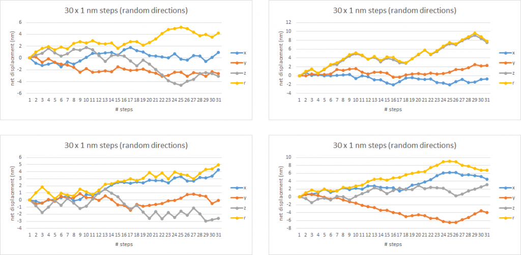
A simple Monte Carlo simulation demonstrates that a fairly wide spread of electron paths is possible even with a low mean free path. In Figure 2, four simulation runs are shown, each representing 30 collisions of an electron, where the electron travels 1 nm in a random direction between collisions (including mostly elastic (no energy lost or gained) and inelastic low energy (<0.1 eV) transfers with phonons [6]), is shown to lead in some cases to travel distances approaching 10 nm. The “r” result is the net distance (regardless of direction) from the original starting point, treated here as (0, 0, 0) , i.e., r=sqrt(x^2+y^2+z^2).
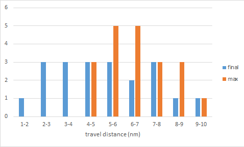
The distribution of distances is shown in Figure 3. The mean final travel distance was 5.1 nm with a standard deviation of 2.25 nm, while the mean max distance was 6.5 nm with a standard deviation of 1.5 nm. Even with a limited sampling (N=20), the distribution of travel distances covers a fairly wide range of nanometers.
Figure 2. Simulations of electrons going through 30 collisions, mostly elastic, the remaining assumed to be low energy transfers to phonons [6].
Figure 3. Distribution of final and maximum travel distances after 20 simulation runs using the conditions of Figure 2.
Increasing or decreasing the travel distance between collisions will naturally increase or decrease the net travel distance as well. The inter-collision distance of 1 nm is comparable to the step size used in other recent related work [7, 8]. Measurements of resist loss from low energy electrons are also in excess of 1 nm [3, 4]. Of course, more collisions accumulated will lead to a wider range of travel distances as well. Another possibility to consider is net positive charge at the starting position, which might slow down further migration by Coulomb force attraction. Recent work, however, suggests this could be negligible [8].
Takeaway Thoughts
For a fully rigorous and complete EUV resist model, in addition to the aerial (photon-only) image input, we need to have the accurate representation of low energy electron blur. These simulation runs hint that it is somewhat oversimplified to have a fixed electron blur value. It is more prudent to consider a range of blur values. This is better for giving the process variation (PV) bands.
Appendix (Technical Note):
Simulations are run on an Excel sheet. Starting point (0, 0, 0). Random spherical coordinate system angle theta (0 to 180 deg) and phi (0 to 360 deg) selected using RANDBETWEEN function, while jump step is fixed (1 nm for this article). Jump = (jump step * sin(theta) * cos(phi), jump step * sin(theta) * sin(phi), jump step * cos(theta)). This is iterated 30 times for the runs in this article.
References
[1] J. Torok et al., “Secondary Electrons in EUV Lithography,” J. Photopolym. Sci. and Tech. 26, 625 (2013).
[2] G. Denbeaux et al., “The role of secondary electrons in EUV resist,” EUVL Workshop 2014.
[3] I. Bespalov et al., “Key Role of Very Low Energy Electrons in Tin-Based Molecular Resists for Extreme Ultraviolet Nanolithography,” ACS Appl. Mater. Interfaces 12, 9881 (2020).
[4] B. Sun, “Low-energy electron-induced chemistry of PMMA,” Master of Science thesis, July 2014.
[5] https://www.linkedin.com/pulse/from-shot-noise-stochastic-defects-dose-dependent-gaussian-chen/
[6] B. Ziaja, R. A. London, and J. Hajdu, “Ionization by Impact Electrons in Solids: Electron Mean Free Path Fitted Over a Wide Energy Range,” J. Appl. Phys. 99, 033514 (2006).
[7] H. Fukuda, “Localized and cascading secondary electron generation as causes of stochastic defects in extreme ultraviolet projection lithography,” J. Micro/Nanolith. MEMS MOEMS 18(1), 013503 (2019).
[8] L. Wiseheart et al., “Energy deposition and charging in EUV lithography: Monte Carlo studies,” Proc. SPIE 9776, 97762O (2016).
Share this post via:


Is Intel About to Take Flight?