
Load-pull power amplifier (PA) design techniques determine the optimal impedances at the power transistor’s extrinsic reference plane, which is the physically accessible boundary for measurement or simulation. This reference plane can be the package transistor leads, die bond pads, or IC chip terminals. It includes the parasitic resistance, capacitance, and inductance inside the GaN device. A simulation-based GaN PA design can supplement this load-pull technique by providing access to the power device’s intrinsic current source. Enhanced GaN models in Keysight’s Advanced Design System (ADS), along with intrinsic techniques like load-line analysis, help RF engineers design high-frequency, highly efficient PAs.
The second webinar session in Keysight’s RF PA design master class series, led by Matt Ozalas, Principal Product Owner for ADS and Scientist, and Joe Schultz, RF Solutions Engineer, explores intrinsic techniques in detail. (The first session focused on extrinsic techniques, particularly load-pull analysis.) Webinar 2 introduces a simple Class J PA design with an intrinsic-node model, examines the history of intrinsic modeling and analysis techniques, and walks through in-depth simulations of the Class J amplifier in an ADS intrinsic analysis workspace.
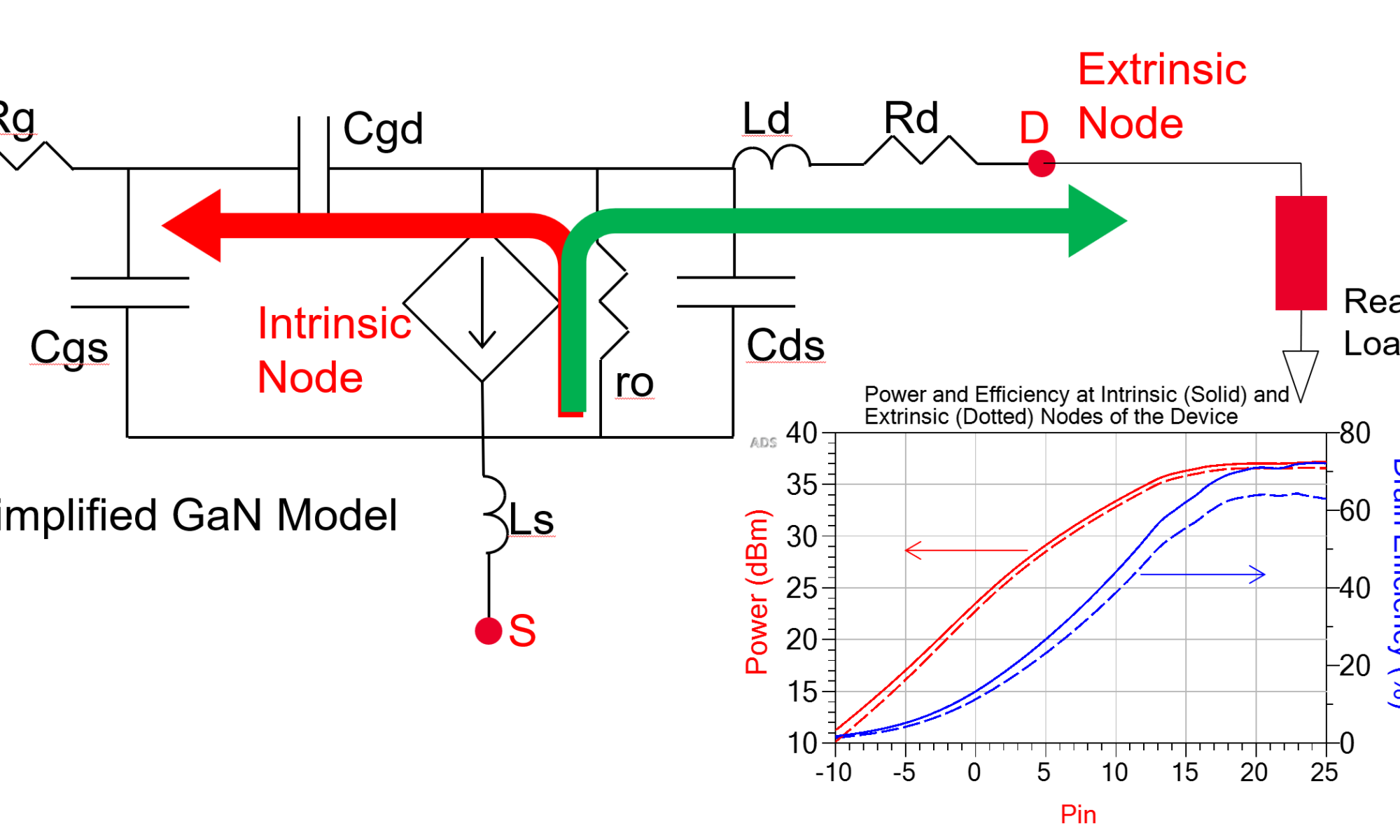
Waveform engineering applied to a Class J PA
An intrinsic node is a virtual construct designed for simulation. Matt starts with a simplified GaN transistor model that surrounds an ideal current generator with non-ideal parasitic elements. Representing parasitics faithfully increases behavior fidelity, which in turn enables a more accurate simulation of efficiency. In the chart below, power tracks between extrinsic and intrinsic analyses, but drain efficiency differs considerably between the two techniques, with the intrinsic analysis being more accurate.

That’s important for a Class J PA, which begins with a construct similar to a Class B amplifier but tunes the harmonic load impedances so that power delivery is zero at the harmonics, theoretically allowing maximum PA efficiency at full voltage swing. Reaching that efficiency requires waveform engineering, strategically reducing the overlap between voltage and current waveforms to minimize resistive power dissipation. “Once we’ve designed these waveforms mathematically, it’s possible to apply a Fourier transform, and then, rather than looking at time-domain waves, we look at harmonic frequency tones,” Matt says. Voltage and current tones at each harmonic frequency yield computed impedances. By applying those Fourier-transformed impedances back to the idealized current generator in the intrinsic transistor model, energy organizes itself to maximize achievable efficiency.
Building comprehensive intrinsic analysis in an ADS workspace
Joe is a recent addition to the Keysight team, with three decades of RF power amplifier design experience spanning Motorola, Freescale, and NXP. He begins with a bit of a digression, mentioning the power amplifier work of Steve Cripps, particularly his 1999 text, “RF Power Amplifiers for Wireless Communications,” and a seminal 2009 article by Paul Tasker on “Practical Waveform Engineering” in IEEE Microwave Magazine.
Joe also shares his own design experience. He worked with Motorola’s LDMOS transistor technology in his early career, which was state-of-the-art at the time. GaN technology can deliver four or five times the power density of LDMOS in amplifier applications, but only if designers pay proper attention to efficiency and power dissipation in PA designs.
After some slides on LDMOS versus GaN, Joe dives into the core of his presentation: a highly technical discussion of an intrinsic approach to RF PA design. The foundation of the analysis is Cripps’ load-line method, which uses swept DC current-voltage (DCIV) analysis with full-scale voltage and current excursions to generate power contours by tracing constant-resistance and constant-conductance circles for different power points on a Smith chart.

Joe also discusses conduction angle, the portion of the RF cycle where current conduction occurs, and one of the differentiators between amplifier classes. The presentation then builds into a GaN FET analysis in ADS, using a new Keysight ASN-HEMT GaN FET demo model and running DCIV, S-parameter, AC sweeps, harmonic balance, and both load-pull and load-line analysis to establish matching impedances. The power of ADS’s data display with the full results is evident in one of Joe’s concluding slides, though a screenshot alone doesn’t do the narrative justice.

If you are interested in RF power amplifier design or learning more about extrinsic load-pull and intrinsic load-line analysis with ADS, hearing from Keysight’s experts makes the time spent viewing these two webinars worthwhile – and yes, the ADS workspaces used in these webinars are available online for hands-on learning. Register for both on-demand sessions at this link:
RF Power Amplifier Design MasterClass Webinar Series
Also Read:
WEBINAR: Two-Part Series on RF Power Amplifier Design
On the high-speed digital design frontier with Keysight’s Hee-Soo Lee
2026 Outlook with Nilesh Kamdar of Keysight EDA
Share this post via:


Comments
There are no comments yet.
You must register or log in to view/post comments.