





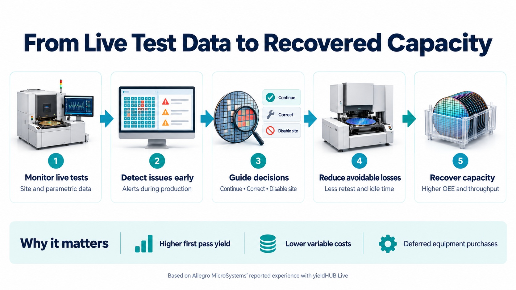



Yesterday at SEMICON West I attended an interesting talk about how to use the masses of die test data to improve silicon yield. The speaker was Dr. Martin Keim, from Mentor Graphics.
First of all, he pointed out that with advanced process nodes (45nm, 32nm, and 28nm), and new technologies like FinFETs, we get design-sensitive defects.… Read More








The $725 Million Chip Development: Why Execution Risk, Not IP Cost, Now Dictates Advanced-Node Survival