Mike Muller, Chief Technology Officer of ARM, has announced the availability of Cortex-A35 processor core for low- to mid-range smartphones at the opening keynote of ARM TechCon on November 10, 2015 in Santa Clara, California. According to Muller, there are going to be 2.8 billion smartphones shipped this year, and more than … Read More
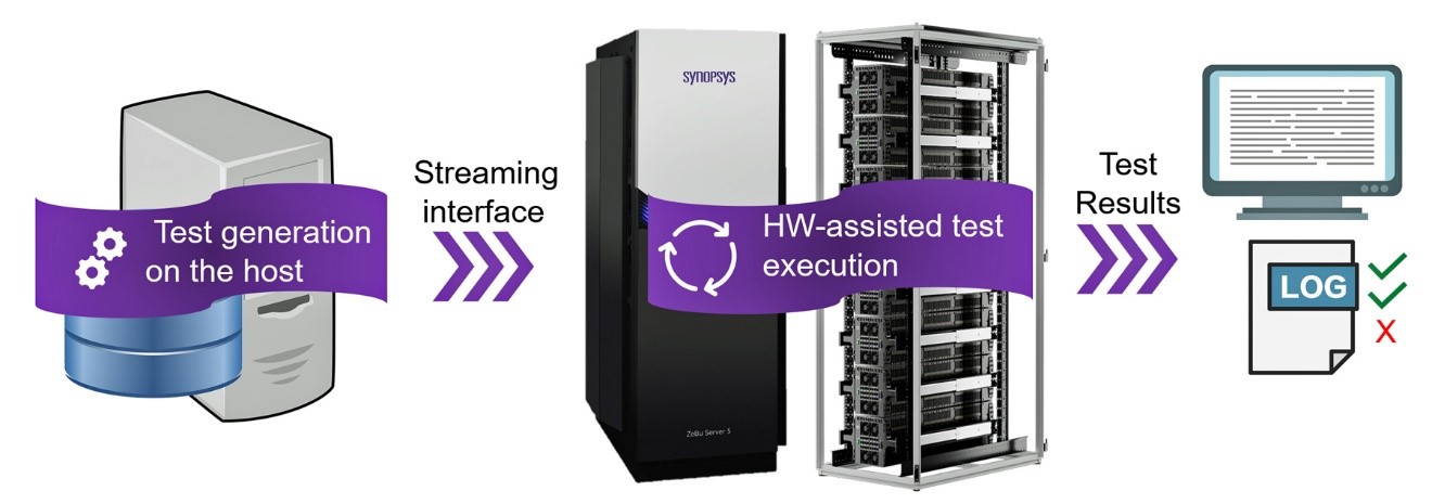 When Software Outruns Silicon: Hardware-Assisted Test Generation to the RescueFor the past decade, the semiconductor industry has…Read More
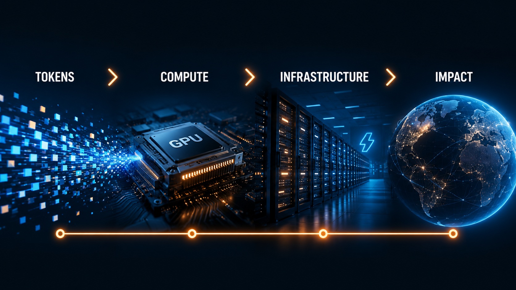 From Tokens to Infrastructure: Why Compute, Memory, and Power Will Determine the Future of AIBased on Dylan Patel’s SEMI Industry Strategy Symposium…Read More
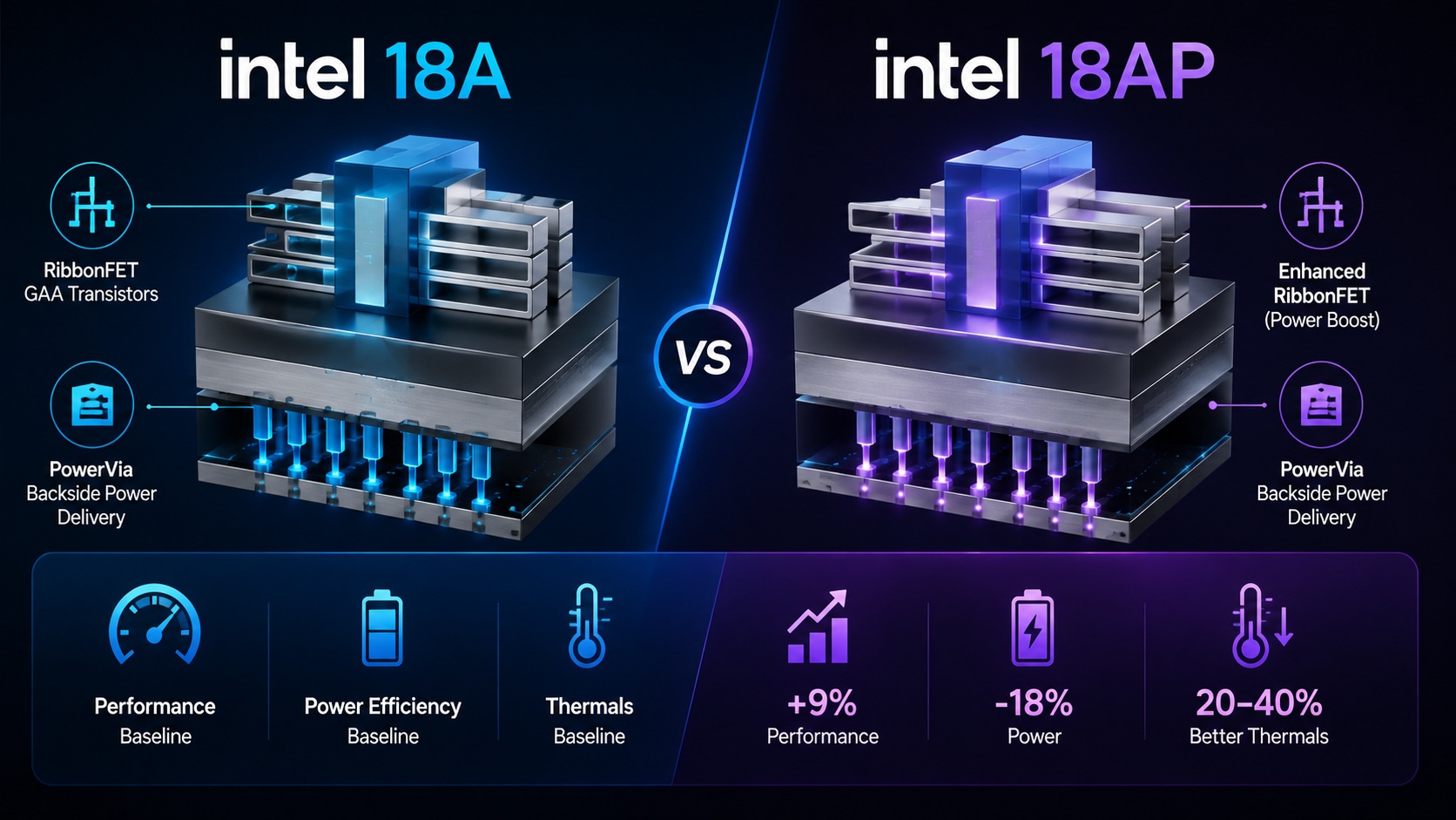 Intel 18A vs Intel 18A-P: What Is the Difference and Why Does It Matter?Intel’s 18A process technology has become one of…Read More
 WEBINAR: Why Google Cloud NetApp Volumes Matter for Modern EDA WorkloadsIn this webinar, Google Cloud and NetApp explore…Read More
 How to Free Yourself from Inconsistent Engineering Documentation Before It’s Too LateEmbedded systems programs often fail because critical engineering…Read More
The Reason ARM Will Win IoT!
After spending the week in Silicon Valley at ARM TechCon and related meetings, there was one common thread amongst the presentations and conversations and that was security. No matter what the topic was, mobile, consumer or industrial IoT, wearables, automotive, etc… security always came up. The question I had was how will companies… Read More
When Talking About IoT, Don’t Forget Memory
Memory is a big enough topic that it has its own conference, Memcon, which recently took place in October. While I was there covering the event for SemiWiki.com I went to the TSMC talk on memory technologies for the IoT market. Tom Quan, Director of the Open Innovation Platform (OIP) at TSMC was giving the talk. IoT definitely has special… Read More
A Novel Microprocessor Fighting Dark Silicon, Energy Efficiency, Code density and Silicon area
Processor cores used in computers and smartphones have become impaired by their own complexity and can’t fully utilize future CMOS generations for increasing their efficiency. Due to the continued increase of density and speed of transistors, these big cores produce too much heat per mm[SUP]2[/SUP] if trying to follow Moore’s… Read More
Merger Mania: The Future of the Semiconductor Industry
In a semiconductor industry which appears maturing, we are also seeing the technologies unravelling newer transistor structures, memories, processors, and newer ways of designing ICs and electronic systems. The present decade appears to be at the cusp of a new transformation in the semiconductor industry. Amid a slew of mergers… Read More
IP-SoC Rebound in 2015 !
Going to IP-SoC every year since 2006, I have enjoyed the conference as it’s the only one 100% IP focused and a very good opportunity to network within this rather small ecosystem of IP vendors… but I must admit that, since 2012, the attendance tend to be lower than before. Because of the well-known “chicken & egg” theorem, low … Read More
HiSilicon’s Experience with Synopsys ICC2

At TSMC’s OIP Symposium last month, Zhe (Jared) Lui of HiSilicon presented their experiences with Synopsys’ ICC2 physical design suite.
Jared started by giving an overview of Huawei and HiSilicon. HiSilicon is the semiconductor arm of Huawei. I assume everyone knows who Huawei is. To a first approximation they … Read More
It’s All about Packaging — In this Material World, Who Is Your Partner?
By Dr. Dan Tracy, senior director, Industry Research and Statistics, SEMI
With the recent release of Apple’s 6s and the form factors of internet-enabled mobile devices and the emergence of the IoT (Internet of Things), advanced packaging is clearly the enabling technology providing solutions for mobile applications and for… Read More
28nm FD-SOI: A Unique Sweet Spot Poised to Grow
I have been silently watching STMicroelectronics pursuing FD-SOI technology since quite a few years. FinFET was anyway getting more attention in the semiconductor industry because of several factors involved. But from a technology as well as economic perspective there are many plus points with FD-SOI. I remember my debate,… Read More
GlobalFoundries Visit – Part 2 – Waking the Sleeping Giant
In part one of this blog I described a visit to GlobalFoundries (GF) Fab 8 site in Malta New York by Daniel Nenni and myself. In this part 2 of the blog, I will describe the second day of our trip when we visited Fab 9 in Burlington Vermont. Before we got to Burlington I thought it would likely be a letdown after seeing the state-of-the-art… Read More
Why Huawei Says It Will Match TSMC’s Most Advanced Chips by 2031