You are currently viewing SemiWiki as a guest which gives you limited access to the site. To view blog comments and experience other SemiWiki features you must be a registered member. Registration is fast, simple, and absolutely free so please,
join our community today!
by Ajay Kumar Govindaram
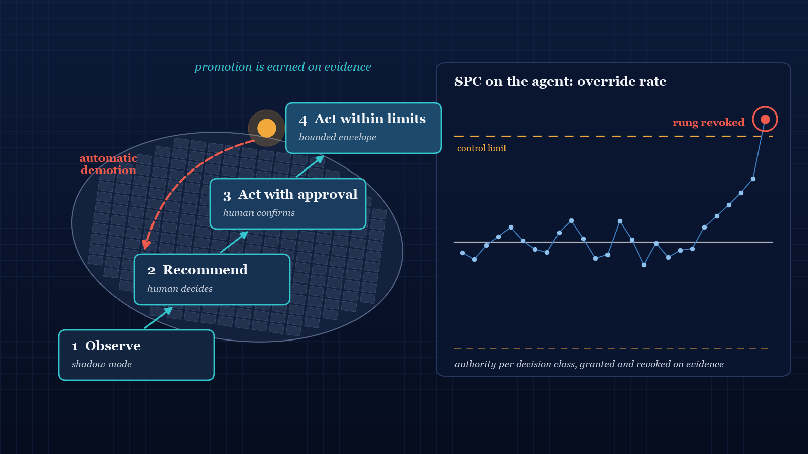
There’s a question I’ve started asking at every agentic AI demo I sit through, and it has a clean answer in every fab on earth: who is allowed to change the recipe? In a semiconductor factory, that was settled decades ago. A person doesn’t touch a production recipe because they feel confident.… Read More
ASML’s decision to collaborate with Xanadu targets one of photonic quantum computing’s most unforgiving engineering constraints: photon loss. The companies will investigate advanced lithography processes for Xanadu’s photonic quantum hardware, focusing on whether tighter patterning control can suppress loss mechanisms… Read More
By Richard Curtin
Ever since the Silicon Catalyst 2023 Semiconductor Industry Forum (“Welcome to our AI Wonderland”) I’ve been convinced that the Nobel Prize committee needs to consider awarding a posthumous award to Sir Arthur.
To remind you, Sir Arthur’s “2001: A Space Odyssey” movie was released in 1968. At that point in time… Read More
At Hot Chips 2026, OpenAI presented Jalapeño, an inference ASIC built with AI in the design loop. As reported from the session by ServeTheHome and Tom’s Hardware, OpenAI showed measured block-level wins over a human baseline — 56% on a BF16 multiply, alongside a 10% smaller matrix-unit area — within a roughly nine-month path from… Read More
Byline: Richard Shreiner
Modern semiconductor architectures are pushing the absolute limits of physical scaling. As data rates climb into sub-picosecond regimes across high-performance computing, 5G/6G infrastructure, and advanced AI clusters, physical layer (Layer 1) signal integrity has shifted from an engineering… Read More
Siemens has announced advances in its collaboration with NVIDIA to accelerate computational lithography, addressing a demanding step in manufacturing advanced AI semiconductors. By integrating NVIDIA’s cuLitho library with Siemens Calibre manufacturing software, the companies aim to make sophisticated photomask optimization… Read More
Francisco Almada Lobo is CEO and co-founder of Critical Manufacturing. He began his career at a CIM research institute and joined Siemens Semiconductors in 1997. In 2004 he led the migration of an MES in a running high-volume facility, and from 2005 to 2009 he managed the Porto Development Center for Infineon and Qimonda, responsible… Read More
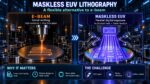
Semiconductor manufacturing depends on lithography: the process of transferring tiny circuit patterns onto a silicon wafer. Conventional extreme-ultraviolet (EUV) lithography projects light with a wavelength of 13.5 nanometers through a reflective optical system, using a custom photomask to define each layer. It can … Read More
Dr. Talluri joined K&S in August 2026 as a member of the Board and assumed the role of President and Chief Executive Officer of K&S in September 2026. Prior to joining K&S, Dr. Talluri served as President, Chief Executive Officer and a member of the Board of Directors at Enovix Corporation, a Nasdaq-listed advanced … Read More
Daniel is joined by Nir Sever, an industry veteran with over 30 years of technological and managerial experience in advanced VLSI engineering. Before joining proteanTecs, Nir served for 10 years as the COO of Tehuti Networks, a pioneer in the area of high-speed networking Semiconductors. Prior to that, he served for 9 years as … Read More











ChipAgent Raises $134Million and Why it Matters