You are currently viewing SemiWiki as a guest which gives you limited access to the site. To view blog comments and experience other SemiWiki features you must be a registered member. Registration is fast, simple, and absolutely free so please,
join our community today!
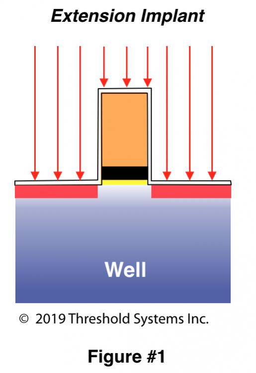
The use of hard masks instead of photoresist for the Extension implant is an effective way to optimize the amount of dopant that is retained along the fin sidewalls for those fins that border along photoresist edges (as discussed in Part 1 of this series).
However, hard masks do nothing to address the dominant problem driving steeper… Read More
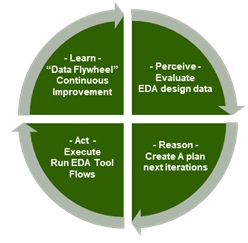
The famous Olympic motto Citius, Altius, Fortius, which is the Latin words for “Faster, Higher, Stronger” to a considerable degree can be adapted to our electronics industry. Traditionally the fundamental metrics we used for measuring the quality of results (QoRs) are performance, power, and area (PPA). Amidst… Read More
At first glance, this seems like a ho-hum topic- just use whatever Arm or RISC-V solution you need – but think again. We’re now expecting to push an awful lot of functionality into these edge devices. Our imaginations don’t care about power, performance and cost; everything should be possible so let’s keep adding cool features.… Read More
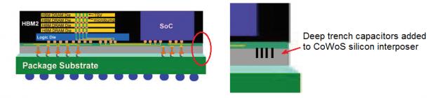
TSMC recently held their annual Technology Symposium in Santa Clara. Part 1 of this article focused on the semiconductor process highlights. This part reviews the advanced packaging technologies presented at the symposium.
TSMC has clearly made a transition from a “pure” wafer-level foundry to a supplier of complex integrated… Read More
Each year, TSMC conducts two major customer events worldwide – the TSMC Technology Symposium in the Spring and the TSMC Open Innovation Platform Ecosystem Forum in the Fall. The Technology Symposium event was recently held in Santa Clara, CA, providing an extensive update on the status of advanced semiconductor and packaging… Read More
The letters “PVT” roll of the tongue easily enough, belying the complexity that variations in process, temperature and voltage can cause for analog designs. For semiconductor processes, there are dozens of parameters that can affect the viability of a design. It would be easy enough to optimize a circuit with only one or two varying… Read More
Methodics has been a key player in IP management for over 10 years. In this section, Methodics shares their history, technology, and their role in developing IP Lifecycle Management (IPLM) solutions for the electronics industry.
Methodics is recognized as a premier provider of IP Lifecycle Management (IPLM) and traceability… Read More
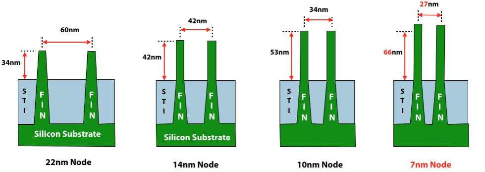
The 3D character of FinFET transistor structures pose a range of unique fabrication problems that can make it challenging to get these devices to yield. This is especially true for the all-important Extension implant that is put in place just prior to the nitride spacer formation.
The Extension implant is a central component of… Read More
Over the last six years EDA has experienced yet another disruption not unlike the Synopsys acquisition of Avant! in 2001 which positioned Synopsys for the EDA lead they still enjoy today. Or the hiring of famed venture capitalist Lip-Bu Tan in 2009 to be the CEO of struggling EDA pioneer Cadence Design Systems. Under Lip-Bu’s… Read More
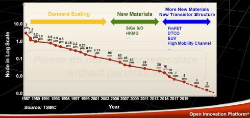
This year TSMC did a FinFET victory lap with the success of 16nm, 12nm, 10nm, and 7nm. It really is well deserved. Even though TSMC credits the ecosystem and customers, I credit TSMC and their relationship with Apple since it has pushed us all much harder than ever before. TSMC CEO C.C. Wei summed it up nicely in his keynote: Innovation,… Read More


Should Intel be Split in Half?