
 The famous Olympic motto Citius, Altius, Fortius, which is the Latin words for “Faster, Higher, Stronger” to a considerable degree can be adapted to our electronics industry. Traditionally the fundamental metrics we used for measuring the quality of results (QoRs) are performance, power, and area (PPA). Amidst the current rise of AI augmented silicon content in many applications, the metrics might need to include the element of “Smartness”. Designed silicon such as cloud or edge based processors and accelerators have shown a trend of faster performance, higher capacity or bandwidth (scalability) and incorporating higher AI content. The smartness level factor may eventually become a key differentiator for the sprouting AI based silicons.
Physical Verification and DRC Rule Explosion
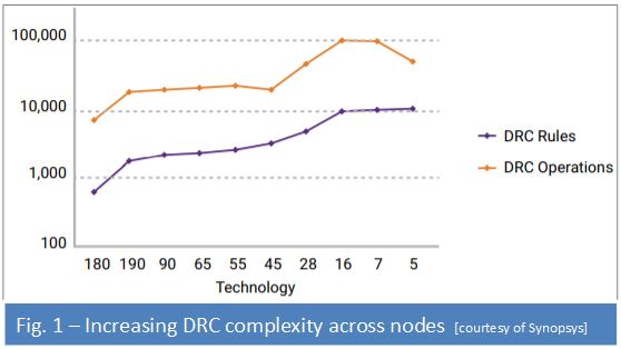 Within the silicon ecosystem, capturing design inceptions into transistor fine geometries involves stepping through several design abstractions and demands successive validations. In many instances, it requires both top-down planning and bottom-up build processes. The similar bottom-up approach gets repeated at the foundry side through the scheme of layered based process implementation. For advanced process nodes, foundries utilize complex front-end-of-line layer stacks and deploy multi-patterning lithography on many masks, which translates to more required masks. Increased overall mask layers (FEOL, MEOL, BEOL) normally implies higher cost and increased complexity for fabrication, backend implementation, and verification.
Elastic Scalability and Cloud Expansion
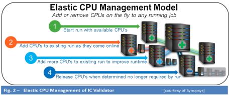
While AI silicon solution track closely to the targeted application or targeted software, in physical verification, the number of process layers and interconnection due to increased pins from emerging applications such as multi-core and AI neural networks have given rise to increased DRC rules to check. In addition, increased embedded IPs to satisfy various data transaction protocols have intensified the demand for more capacity expansion. Synopsys IC Validator physical verification has an intelligent scheduler, which is an essential feature for its elastic scalability. The smart load sharing technology regularly monitors jobs and determines job health. Based on the job needs and the compute server constraints, it will make on-the-fly adjustment to subsequent CPU cores addition or removal.
The memory-aware scheduling also estimates memory requirements in advance and schedules jobs based upon the requested hardware configurations. It enables optimal utilization of compute farms available resources for physical verification jobs, regardless of the current off-peak or max-peak state. It leaves control to designers to align with their project schedule demand. For example, given an IC validator job requiring 100 CPUs, it may take the first 10 available CPU for use and dynamically add more CPUs as they become available. Similarly, it could free-up some CPUs as the job is nearing completion if need be, as illustrated in figure 2.
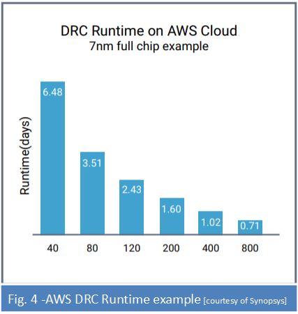
IC Validator has also been enabled to be a “cloud-ready” physical signoff solution and has been deployed on the cloud for production tapeouts. The chart illustrates the runtime of a production 7nm design can be scaled down to less than a day with scaled cores on AWS.
Steps to Ensure Convergence
From the methodology standpoint, there are three approaches available to improve physical verification productivity:
• Run concurrently during the IP and block-level design capture.
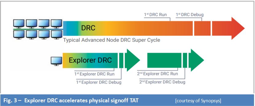
Using physical verification Fusion, DRC and manufacturing issues are caught much earlier in the design cycle, reducing or eliminating late-stage surprises close to tapeout. IC Validator’s seamless integration with Fusion Compiler and IC Compiler II enables layout auto-correction interface –which identifies DRC violations such as DPT decomposition violations and initiates automatic repairs. The applied corrections are then validated with signoff foundry runsets using IC Validator Physical verification, further eliminating iterations. This will allow block owners to identify potential failures while the design is still being edited, incurring smaller validation cycle. The DRC run will take seconds to complete and available for a quick fix as the layout view tool has been streamlined with IC Validator Live DRC engine.
• Run full-chip verification on early integrated design version.
Today’s SoC’s consist of numerous blocks, spanning from mixed-signals cells, memory, third-party IP’s and I/O cells. IC Validator Explorer DRC is capable of providing a quick assessment of the full-chip design and provides actionable feedback to fix found problems. As each block may get validated in a bottom-up fashion, when compiled into a full-chip level, additional problems might surface, such as missing blockages, misalignment issue, and block revision controls to name a few.
Designers could utilize IC Validator Explorer DRC to quickly prescreen the full design using a baseline set of DRC rules to gauge the design readiness prior to a full-blown signoff check. If the outcome is relatively clean, it will continue to progressively complete all required DRC signoff checks. This full-chip approach was found to deliver 5X faster runtime at 5X fewer cores versus the traditional approach, which translates to a few needed hours for typical full chip 7nm designs with 16 or 32 cores. A dramatic improvement, even when it is still considered in ‘dirty state’.
• Run on more CPU resources.
The third option is to provide room for scalability to take place. 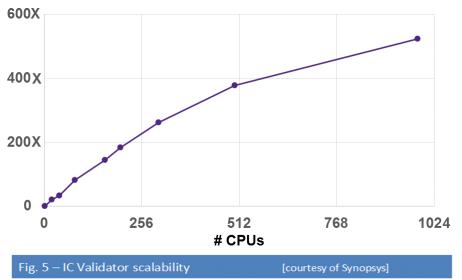 As IC Validator scalability index indicates quite effective CPU utilization, overall job sign-off speedup could be attained through core expansion.
Integrated Analytic Facilities at Chip and Block Levels
To easily identify the macro-problems to fix (such as overlaps), IC Validator includes an error heatmap visual topological assessment. The color gradient heatmap shows various hot spots intensity starting from high (in red), progressing to cool areas (in blue) –analogous to the congestion hot-stop in P&R.
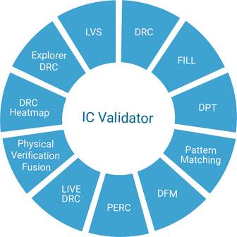
All of the above-described measures work in tandem to deliver convergence to physical design signoff. For more details on IC Validator please refer check HERE.
Share this post via:


Comments
There are no comments yet.
You must register or log in to view/post comments.