
This morning, Synopsys announced its new Die-to-Die PHY IP. This announcement is critically important as it addresses two major market drivers – the growing need for faster connectivity in the datacenter and similar markets, and a path to better exploit the latest processes by dealing with yield issues for larger dies in a different manner. Also, this seems to be just the first step in this area, and we will anxiously await further advances in die-to-die connectivity. I believe Synopsys is trying to take the lead here and potentially help drive for industry standards that do not yet exist. Please read the press release for the details. Below, I will focus on what solutions this announcement can enable for use by chip architects and designers.
I have written a few times in the past few months on SerDes and other high-speed connectivity paths in the datacenter. Given the seemingly ever-growing demands for cloud computing, whether in e-commerce, machine learning, AI, gaming – the list is growing daily – datacenter administrators are hungry to find ways to deliver high performance. This pursuit has seen many gains in PCIe (inside the chassis), computer-to-computer, rack-to-rack, and datacenter-wide areas. High-speed optical solutions are now targeting high-speed in lengths up to 10 km. But these solutions still come with some latency and area penalties that make them prohibitive for a die-to-die solution.
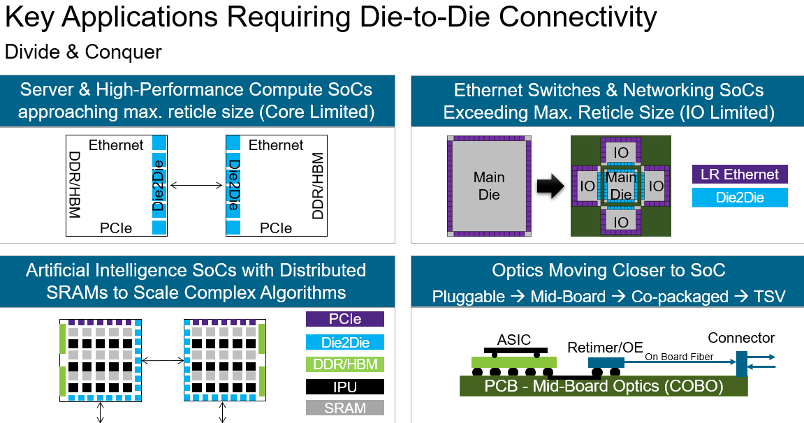
By being able to connect multiple dies on a substrate in a point to point manner using the new Synopsys die-to-die PHY, which is available now, you can create a larger piece of functionality with less latency between the blocks. Admittedly, there has not been enough standardization for this type of solution. BGA-style connections within multi-chip modules (MCM) are not new, but there has not been much standardization of the PHYs connecting them. Initially, this solution will only be available on a single 7nm FinFET process, so it doesn’t yet support a heterogenous MCM solution. However, I expect that will certainly be coming soon. For now, this advancement alone is impressive.
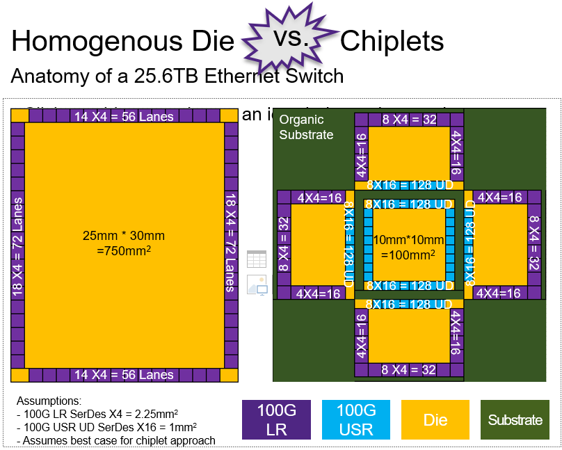
As you make larger and larger semiconductor dies on the latest manufacturing processes, yield usually drops dramatically which significantly increases cost. If you take that same design and split it into multiple smaller dies in the same process you can see a huge saving in cost just from the improved yield. To achieve lower cost, the saving from the yield need only be more than the additional cost of the substrate used to connect the dies. If the original die was already going to sit on a substrate, then this is an easy decision. If not, it is still an option worth exploring as it may very well be less expensive to produce.
Another interesting consideration is what this technology can enable in conjunction with other technologies. For example, I can envision a design where multiple chiplets are placed in a row on a substrate forming a datapath (e.g., data flowing left to right, from die to die). If you need chunks of nearby memory, you have a choice, north or south of the datapath elements on the substrate, or can you place the memory on top of the datapath element, perhaps using another substrate? In other words, can you have BGA connection above and below the die? It is an interesting thought. Of course, that may also bring up thermal and other EM considerations. The use of stacked die is not a new thought. So how far can we take this new development from Synopsys? My imagination is started to run wild.
“1.8 terabit-per-second per millimeter unidirectional bandwidth for high throughput die-to-die connectivity.”
“One picojoule per bit (pJ/bit) for ultra-low-power.”
What will designers due with that? We should all be excited to find out.
Share this post via:


Comments
One Reply to “Synopsys’ New Die-to-Die PHY IP – What It Means”
You must register or log in to view/post comments.