Array
(
    [content] => 
    [params] => Array
        (
            [0] => /forum/index.php?threads/tsmc-az-update.19999/
        )

    [addOns] => Array
        (
            [DL6/MLTP] => 13
            [Hampel/TimeZoneDebug] => 1000070
            [SV/ChangePostDate] => 2010200
            [SemiWiki/Newsletter] => 1000010
            [SemiWiki/WPMenu] => 1000010
            [SemiWiki/XPressExtend] => 1000010
            [ThemeHouse/XLink] => 1000970
            [ThemeHouse/XPress] => 1010570
            [XF] => 2021370
            [XFI] => 1050270
        )

    [wordpress] => /var/www/html
)

TSMC AZ Update

Daniel Nenni

Admin
Staff member
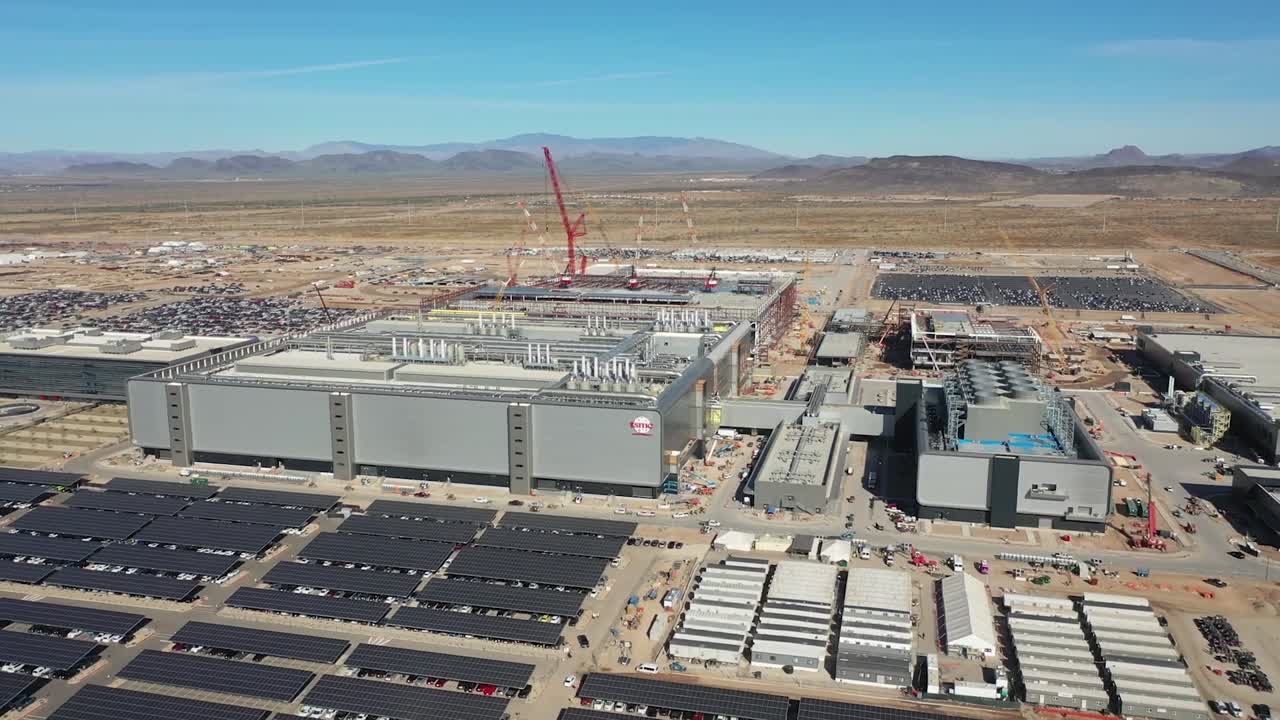
TSMC Arizona’s first fab is on track to begin production leveraging 4nm technology. The second fab will produce the world’s most advanced 2nm process technology with next-generation nanosheet transistors in addition to the previously announced 3nm technology. Our newly announced third fab will produce chips using 2nm and/or more advanced processes, with production beginning by the end of the decade. Each of the three fabs, like all of TSMC’s advanced fabs, will have cleanroom area approximately double the size of an industry standard logic fab.

Through increasing our capacity for leading-edge technology at TSMC Arizona, we will be supporting our customers unleash innovations in all different fields including mobile, AI and HPC.

Watch this video to understand more about the exciting innovations we will make possible in Phoenix, Arizona.

 
4nm is late by a year, it is N-2 clearly not leading edge in US.

Phase 2 will do both N3 and Nanosheet, the two flows are so different hard to believe there will be anything but a small pilot line that bait the press and politicians.

Phase 3 by 2030, that will be at best N-2.

Taiwan and TSMC keeping the Crown Jewels and volume at home
 
4nm is late by a year, it is N-2 clearly not leading edge in US.
Phase 2 will do both N3 and Nanosheet, the two flows are so different hard to believe there will be anything but a small pilot line that bait the press and politicians.
Phase 3 by 2030, that will be at best N-2.
Taiwan and TSMC keeping the Crown Jewels and volume at home

You need to look at revenue per node which is what fills a fab. N5/4 is still the big money maker for TSMC and the difference between N4 and N3 fabs is minor so you can make N3 in an N4 fab when utilization drops.

How do you know N3 and N2 fabs are so different? Are you guessing or do you actually know? I have been told otherwise.

Having N4, N3, and N2 in AZ is very strategic and customer driven. TSMC builds based on customer request. This is not a "build it and they will come" scenario. If customers needed N4 in AZ sooner it would have been done sooner.
 
4nm is late by a year, it is N-2 clearly not leading edge in US.

Phase 2 will do both N3 and Nanosheet, the two flows are so different hard to believe there will be anything but a small pilot line that bait the press and politicians.

Phase 3 by 2030, that will be at best N-2.

Taiwan and TSMC keeping the Crown Jewels and volume at home
Not true. The press release states "the third fab will produce chips using 2nm or more advanced processes". Also TSMC has repeatedly moved the plans to more advanced nodes with each new update, so I'm not sure why you are so sceptical. It was originally only a N7 site, then went to 6N, then the plan changed to N5 and then N4. Now its a N4, 3N, 2N site. Not sure why it hard to believe 1.4N will not be added as well?
 
Not true. The press release states "the third fab will produce chips using 2nm or more advanced processes". Also TSMC has repeatedly moved the plans to more advanced nodes with each new update, so I'm not sure why you are so sceptical. It was originally only a N7 site, then went to 6N
That is derivative nodelet. TSMC almost never converts fabs to new process technologies, they almost always build new fabs for new process node families. The only exceptions in TSMC company history are 20nm fabs since that technology didn't gain widespread adoption, 10FF for the same reason, and recently TSMC mentioned converting some of their Fab 18 equipment to N3 to avoid an N7 underutilization problem. Long term I also just assume that TSMC will move all N5 customers to N3 just like how they are trying to move everyone on planar to 28nm, 28nm folks to 16FF, and 16FF folks to N7 family.
then the plan changed to N5 and then N4.
No it didn't N5/4 started in the newly built fab18. N7 family has never run there and never will. Also N4 is just a 2% optical shrink. If you mean Fab 21, then it was always marketed as an N5/4 fab for P1 and N3 for P2
Now its a N4, 3N, 2N site. Not sure why it hard to believe 1.4N will not be added as well?
Maybe P4 maybe P3. Depends on how much equipment crossover there is with N1.4. If it is a lot then they could just convert it, but my bet is that P4 will just be built as N1.4 and maybe they flex some gear around as N2/N1.4 demand changes.

How do you know N3 and N2 fabs are so different? Are you guessing or do you actually know? I have been told otherwise.
BEOL is likely the same, and there are likely similarities with FEOL, but there are likely a ton of added tools for GAA (and a larger ratio of FE vs BE if we assume the metal stacks are the same). Also there are then the extra tools for BSPDN formation. My guess is that N2 will share alot in common with N1.4 rather than N5/N3. If N1.4 is a bigger jump so that a bunch of N3 folks can justify jumping ship (I think it will be a similar to what is happening with N5 deramp powering up the N3 ramp). But maybe it ends up being more like SF1.4 and it is a very small jump. If that is the case, then I would be super confident thant N1.4 and N2 would share many tools (and that N1.4 will just flat out replace N2 just like how 10FF replaced N7).
 
That is derivative nodelet. TSMC almost never converts fabs to new process technologies, they almost always build new fabs for new process node families. The only exceptions in TSMC company history are 20nm fabs since that technology didn't gain widespread adoption, 10FF for the same reason, and recently TSMC mentioned converting some of their Fab 18 equipment to N3 to avoid an N7 underutilization problem. Long term I also just assume that TSMC will move all N5 customers to N3 just like how they are trying to move everyone on planar to 28nm, 28nm folks to 16FF, and 16FF folks to N7 family.

No it didn't N5/4 started in the newly built fab18. N7 family has never run there and never will. Also N4 is just a 2% optical shrink. If you mean Fab 21, then it was always marketed as an N5/4 fab for P1 and N3 for P2

Maybe P4 maybe P3. Depends on how much equipment crossover there is with N1.4. If it is a lot then they could just convert it, but my bet is that P4 will just be built as N1.4 and maybe they flex some gear around as N2/N1.4 demand changes.


BEOL is likely the same, and there are likely similarities with FEOL, but there are likely a ton of added tools for GAA (and a larger ratio of FE vs BE if we assume the metal stacks are the same). Also there are then the extra tools for BSPDN formation. My guess is that N2 will share alot in common with N1.4 rather than N5/N3. If N1.4 is a bigger jump so that a bunch of N3 folks can justify jumping ship (I think it will be a similar to what is happening with N5 deramp powering up the N3 ramp). But maybe it ends up being more like SF1.4 and it is a very small jump. If that is the case, then I would be super confident thant N1.4 and N2 would share many tools (and that N1.4 will just flat out replace N2 just like how 10FF replaced N7).
I’m aware of the nodlets. I was referring to the change in scope of the site as a whole. It was initially just going to be a N7 site. And then it changed to N5. And then N5 changed to N4 nodlets. They did move the base process technology they are going to produce there up in complexity each time and aren’t going to be producing some outdated node there was my point. They seem committed to relatively close to leading edge.
 
Last edited:
As Daniel said, TMSC does not build fabs on spec. If they are planning to build an N2 fab in AZ, that means they have customer committed volumes for it - it would not be some kind of pilot line for demonstration purposes. And they will probably build an N2 fab in Taiwan first, so yes they will keep the crown jewels at home - why would anyone expect otherwise?
 
As Daniel said, TMSC does not build fabs on spec. If they are planning to build an N2 fab in AZ, that means they have customer committed volumes for it - it would not be some kind of pilot line for demonstration purposes. And they will probably build an N2 fab in Taiwan first, so yes they will keep the crown jewels at home - why would anyone expect otherwise?

I think it is funny that the Apple CEO is all for TSMC AZ but since Apple is first to a node most of their production will stay in Taiwan. I know the Apple products have a life beyond 2 years but the majority share is done in the first two years, my opinion. I'm talking about iPhones not Macs.
 
That is derivative nodelet. TSMC almost never converts fabs to new process technologies, they almost always build new fabs for new process node families. The only exceptions in TSMC company history are 20nm fabs since that technology didn't gain widespread adoption, 10FF for the same reason, and recently TSMC mentioned converting some of their Fab 18 equipment to N3 to avoid an N7 underutilization problem. Long term I also just assume that TSMC will move all N5 customers to N3 just like how they are trying to move everyone on planar to 28nm, 28nm folks to 16FF, and 16FF folks to N7 family.

As I remember it, TSMC 20nm was the first step (double patterning) to FinFETs and it does use the same fabs as 16nm. Since 10nm didn't have EUV it was not fitted for N7.
 
Personally I think Moores law is slowing down - even for TSMC - so the life of nodes will extend a bit. It also makes sense for TSMC to do their yield learning in Taiwan where they are closer to their core engineering teams and there is a better manufacturing culture.
 
As Daniel said, TMSC does not build fabs on spec. If they are planning to build an N2 fab in AZ, that means they have customer committed volumes for it - it would not be some kind of pilot line for demonstration purposes. And they will probably build an N2 fab in Taiwan first, so yes they will keep the crown jewels at home - why would anyone expect otherwise?

Based on the design starts I have seen thus far N2 will be another big node. Not as big as N3 (no Intel) but big so N2 in AZ makes sense. N2 and N1.4 will be cousins so the same fab, my guess.
 
As I remember it, TSMC 20nm was the first step (double patterning) to FinFETs and it does use the same fabs as 16nm. Since 10nm didn't have EUV it was not fitted for N7.
Daniel: It seems not work on the way you think. As mentioned by CC Wei or other tsmc executives before, the tools are reused heavily between advanced nodes. Typically it will be 90% or higher. For Foundry, it takes longer time in process/product qualification for fab node conversion. 20nm and 16nm used the same BEOL DR, the difference is transistor architecture changed from planar to FinFET. Planar device nearly hit the device leakage and other electostatistic limits, there is no surprise that 20nm demised with time. tsmc used the same HVM fab (Fab15) for 10nm and 7nm, even 6nm nodes. The early version of 7nm did not have EUV layers. But when EUV layers development were ready in 7nm, there were several EUV scanners introduced into that Fab to support the requirements. I guess the 10nm and 7nm re-use rate would be >98%.
 
Daniel: It seems not work on the way you think. As mentioned by CC Wei or other tsmc executives before, the tools are reused heavily between advanced nodes. Typically it will be 90% or higher. For Foundry, it takes longer time in process/product qualification for fab node conversion. 20nm and 16nm used the same BEOL DR, the difference is transistor architecture changed from planar to FinFET. Planar device nearly hit the device leakage and other electostatistic limits, there is no surprise that 20nm demised with time. tsmc used the same HVM fab (Fab15) for 10nm and 7nm, even 6nm nodes. The early version of 7nm did not have EUV layers. But when EUV layers development were ready in 7nm, there were several EUV scanners introduced into that Fab to support the requirements. I guess the 10nm and 7nm re-use rate would be >98%.

From what I remember a fab must be specifically built for EUV, to house the EUV systems. Non EUV fabs will not work structurally. 10nm was an EUV ready fab? TSMC 7nm was a big node. 7nm+ EUV not so much but 6nm is big and has EUV. It looks to me like the High NA EUV systems are actually smaller so that should not be a problem moving forward.
 
From what I remember a fab must be specifically built for EUV, to house the EUV systems. Non EUV fabs will not work structurally. 10nm was an EUV ready fab? TSMC 7nm was a big node. 7nm+ EUV not so much but 6nm is big and has EUV. It looks to me like the High NA EUV systems are actually smaller so that should not be a problem moving forward.
The trick is there are several " new phases" in each fab cluster which are interoperable. It should be planned well ahead for expansion and future requirements.
 
Back
Top