Array
(
    [content] => 
    [params] => Array
        (
            [0] => /forum/index.php?threads/the-battle-on-advanced-processes-intensifies-as-asml-plans-to-produce-ten-equipment-capable-of-2nm-chip-production-next-year.19340/
        )

    [addOns] => Array
        (
            [DL6/MLTP] => 13
            [Hampel/TimeZoneDebug] => 1000070
            [SV/ChangePostDate] => 2010200
            [SemiWiki/Newsletter] => 1000010
            [SemiWiki/WPMenu] => 1000010
            [SemiWiki/XPressExtend] => 1000010
            [ThemeHouse/XLink] => 1000970
            [ThemeHouse/XPress] => 1010570
            [XF] => 2021370
            [XFI] => 1050270
        )

    [wordpress] => /var/www/html
)

The Battle on Advanced Processes Intensifies as ASML Plans to Produce Ten Equipment Capable of 2nm Chip Production Next Year

Daniel Nenni

Admin
Staff member

EUV-system-in-Final-Assembly_48557-624x416.jpg


As TSMC, Samsung, and Intel compete fiercely in the race for 2nm advanced processes, a new wave of the “battle for crucial equipment” is simultaneously unfolding.

According to South Korean reports, ASML, the leader in semiconductor advanced lithography equipment, plans to manufacture ten equipment capable of producing 2nm chips next year, while aiming to increase its annual production capacity to 20 devices in the coming years.

Intel has secured up to six of the 10, taking the lead, while Samsung is also actively pursuing the procurement of the equipment. TSMC faces significant pressure in this competitive landscape.

South Korean tech media SamMobile has unveiled that as major semiconductor manufacturers announce plans to start producing 2nm chips in 2025, ASML is set to unveil equipment capable of manufacturing chips using the 2nm process in the coming months.

The latest extreme ultraviolet (EUV) lithography equipment is expected to increase the numerical aperture (NA) from 0.33 to 0.55. This enhancement improves the light-collecting capability of the optical system, enabling semiconductor fabs to utilize advanced patterning techniques for the production of 2nm process chips.

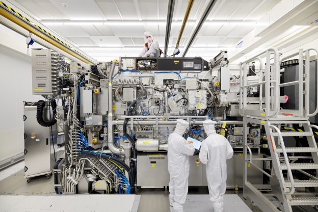
ASML is the sole global manufacturer of advanced EUV equipment for processes at 7nm. These equipment are not only expensive, costing several million dollars each, but they also have limited production capacity.

It has led to high demand from major semiconductor manufacturers like Samsung, Intel, and TSMC. Currently, only five chipmakers globally, including TSMC, Samsung, SK Hynix, Intel, and Micron, require EUV equipment, with TSMC accounting for 70% of EUV purchases.

Consequently, Samsung is actively pursuing collaboration and has signed a historic agreement with ASML to jointly invest KRW 1 trillion (approximately USD 755 million) in establishing a research and development facility in South Korea.

This collaboration aims to contribute to the development of Samsung’s 2nm process. Samsung plans to commence the production of 2nm process chips by the end of 2025 after acquiring the 2nm manufacturing equipment.

Samsung Electronics Vice Chairman Kyung Kye-hyun, who heads the Device Solutions Division, emphasized that the new agreement with ASML will assist Samsung in acquiring the next-generation high NA EUV equipment.

Kyung said, “Samsung has secured a priority over the High-NA equipment technology. (From the trip), I believe we created an opportunity for us to optimize the usage of High-NA technology for our production of DRAM memory chips and logic chips in the long term.”

On the Intel front, as part of its IDM 2.0 strategy, it is executing a 5 nodes in four years process development plan. Intel emphasizes that its Intel 20A process is progressing towards volume production readiness as planned, while the Intel 18A process is scheduled to test production phase in the first quarter of next year.

Facing the strong competition from Samsung and Intel, TSMC is not sitting idle. According to reports citing from Financial Times, TSMC has showcased its 2nm prototype test results to major clients like Apple and NVIDIA.

TSMC previously mentioned in its earnings call that it expects the 2nm process to enter mass production as scheduled in 2025. The company’s 2nm backside power rail solution is scheduled for the latter half of 2025, with mass production slated for 2026.

(Photo credit: ASML)

 
More from Kyung: https://www.koreaherald.com/view.php?ud=20231215000518

According to Kyung, Samsung and ASML will build a joint research facility in Dongtan, Gyeonggi Province and bring the High-NA EUV equipment into the facility. There, the engineers of the two companies will work together to enhance the chipmaking process, Kyung said.

"Rather than focusing on how fast we bring the High-NA EUV machine into Korea, it is more important for us to build the partnership (with ASML) so that Samsung can better use the next-generation equipment," Kyung said, adding that Samsung did forge a strong partnership with a very "sturdy ally."
 
Intel has secured up to six of the 10, taking the lead, while Samsung is also actively pursuing the procurement of the equipment. TSMC faces significant pressure in this competitive landscape.

I'm checking into this. TSMC is ASML's #1 customer so it would surprise me if Intel cut in line for NA EUV without TSMC knowing/planning for it. It might be that TSMC can go A14/N1 without NA EUV which would be a big cost saver.
 
I'm checking into this. TSMC is ASML's #1 customer so it would surprise me if Intel cut in line for NA EUV without TSMC knowing/planning for it. It might be that TSMC can go A14 without NA EUV which would be a big cost saver.
Nothing seems odd about this to me. ASML doesn’t discriminate or pick favorites. It is also in their interest to make sure intel doesn’t drop out of leading edge as that gives other manufacturers more pricing power. IF this story is true, my guess is intel 6, TSMC and Samsung 2 each. Not a huge difference in the grand scheme of things.

I don’t think it is a big deal either way. In my opinion I don’t think the industry will see significant pitch scaling until we get to TMDs, better etch/dep hardware, and new metallization techniques. I think that if it wasn’t for the backside of the wafer, CFETs, etc we would enter a more DRAM like logic industry with small cost effective shrinks and improved power-performance characteristics. I think that the big density improvements are only going to be coming from architectural innovations.
 
What about the rest of the equipment required to produce a 2nm chip?

That all off the peg stuff that anyone can make?

This obsession with ASML Lithography tools would imply its all you need.
 
What about the rest of the equipment required to produce a 2nm chip?

That all off the peg stuff that anyone can make?
I wouldn’t go that far. If it was easy more folks would do it.
This obsession with ASML Lithography tools would imply its all you need.
I assume that isn’t directed at me, since I have been very consistent in my narrative that all of the other stuff is exactly important and that better litho is worthless without better etch and dep hardware (especially when we are talking GAA and the like).
 
I wouldn’t go that far. If it was easy more folks would do it.

I assume that isn’t directed at me, since I have been very consistent in my narrative that all of the other stuff is exactly important and that better litho is worthless without better etch and dep hardware (especially when we are talking GAA and the like).

I am talking in general... any article on Semiconductor equipment/material requirements, starts an ends with ASML in almost all mainstream media.
They talk as if thats all you need while indirectly minimising the contributions of other areas. Thats why I made my off the peg comment.
Just annoys me a bit.
 
What about the rest of the equipment required to produce a 2nm chip?

That all off the peg stuff that anyone can make?

This obsession with ASML Lithography tools would imply it’s all you need.
Lithography has always been the technical driver the shrink gate width. Remember that TSMC’s early adoption of EUV was what allowed them to surpass Intel in manufacturing the most advanced semiconductor devices. It’s all about who can get the latest lithography into production.
 
Lithography has always been the technical driver the shrink gate width.
Yeah in the Dennard era it was. Litho hasn't been the main bottleneck on gate shrinkage in the post Dennard era. If you are saying this it is clear you aren't super familar with semi manufacturing (especially with GAA processes). If you would like to learn more about the criticality of the rest of the things that make those EUV machines useful rather than paper weights, there are some super accessible articles on IEEE.Spectrum, semiengineering, and a few on semiwiki from the more process adjacent authors like Fred chen. Obviously they have an agenda, but you can also find some nice marketing papers from AMAT, TEL, Lam, etc on the challenges of GAA nodes. If your institution has access you can learn a lot more about the beyond litho parts of patterning from such conferences as SPIE.
Remember that TSMC’s early adoption of EUV was what allowed them to surpass Intel in manufacturing the most advanced semiconductor devices.
Not really. N7/N7P didn't use EUV, and N7+/N6 barely used EUV to the point of its only purpose was to derisk N5. If EUV was the only thing that mattered why didn't Samsung leap ahead of TSMC? They fully embraced EUV 2 years before TSMC did.
It’s all about who can get the latest lithography into production.
No. For one it needs to be cost effective. Samsung was first, but it didn't matter because it wasn't HVM ready yet so early 7LPP production volume was pitiful. Another example of this would be if you tried to shrink TSMC 90nm to a ~47pp like N3B. For one the performance would suck. But more importantly the active power would be super high, and leakage would be so bad you couldn't even tell if the transistor is even on.
 
Mr. Ng, can you please make a prediction of what the post GDS2/OASIS NRE cost will be to the customer 2 and 4 years from today.

1) The classic 16nm: With routable contacts + double patterned M3 and below + M4-M8 at 2x + M9-M10 at 4x + M11-M2 wide + M13 API

and

2) 6nm (One that uses EUV up to M4 you mentioned a year or so ago) with an equivalent metal stack

3) Any process that you would recommend to a cellphone manufacturer

I trust your judgement over the chart followers.
 
Mr. Ng, can you please make a prediction of what the post GDS2/OASIS NRE cost will be to the customer 2 and 4 years from today.
No clue what post GDS2 or OASIS means and I have no clue what NRE costs would be for any node. All I can presume is that for newer nodes NREs go up faster than the wafer cost does (note cost not price since that is dependent on non technical considerations). I also have no clue what premium mask shops/eda guys charge above said NRE cost.
 
Post GDS2/OASIS means sending the files off to have the OPC and masks made. Avoid the prediction of the mask making cost. How about the fab charges?

To argue the merits of going to these 6nm and below processes, isn't a prediction of the NRE cost needed? You know the etchers, the process steps, etc, correct?

Cost estimations are easier to predict than revenue projections.

Anybody else want to make a prediction?
 
Last edited:
Post GDS2/OASIS means sending the files off to make the masks made. Avoid the prediction of the mask making cost. How about the fab charges?
NRE is just the cost of a couple of wafers, mask making, and the design services from your foundry; yes? If so I can only really speak to the cost of making said wafers. Mask writing and services is not something I have any visibility into.
To argue the merits of going to these 6nm and below processes, isn't a prediction of the NRE cost needed?
Yes that info is needed. But I can only speak about what I know. What I know is from a wafer cost and a cost per FET perspective. From my perspective the new node should generally be more cost effective after the first year or two than all prior nodes (but the premium that foundries want to charge over cost can certainly mess with that generally true statement depending on how large said premium is). It is also important to remember I work at a firm that produces its products in VERY LARGE volumes. For products like that total product cost is dominated by the cost per good die.
You know the etchers, the process steps, etc, correct?
Yes, but even if I knew the exact structural cost of TSMC's process technologies, that doesn't mean I know what price TSMC is going to be charging you.
 
Back
Top