Array
(
    [content] => 
    [params] => Array
        (
            [0] => /forum/index.php?threads/tech-war-china-quietly-making-progress-on-new-techniques-to-cut-reliance-on-advanced-asml-lithography-machines.19941/
        )

    [addOns] => Array
        (
            [DL6/MLTP] => 13
            [Hampel/TimeZoneDebug] => 1000070
            [SV/ChangePostDate] => 2010200
            [SemiWiki/Newsletter] => 1000010
            [SemiWiki/WPMenu] => 1000010
            [SemiWiki/XPressExtend] => 1000010
            [ThemeHouse/XLink] => 1000970
            [ThemeHouse/XPress] => 1010570
            [XF] => 2021370
            [XFI] => 1050270
        )

    [wordpress] => /var/www/html
)

Tech war: China quietly making progress on new techniques to cut reliance on advanced ASML lithography machines

Daniel Nenni

Admin
Staff member
- By applying SAQP to DUV machines, China could make sophisticated 5-nanometre grade chips without the need for more advanced EUV tools sold only by ASML
  • - Local semiconductor equipment leader Naura Technology Group began preliminary research into lithography systems in March, according to sources
NAURA China Tec.jpg

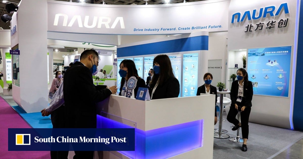
Beijing-based Naura Technology Group started research on lithography systems last month, according to people familiar with the matter, as China’s home-grown semiconductor tool makers try workarounds to produce advanced chips without the latest equipment from Dutch giant ASML, a breakthrough that could potentially thwart US attempts to contain China’s chip-making capabilities.

The efforts, which involve multiple players in China’s semiconductor supply chain, have made preliminary research progress, with a patent application by Huawei Technologies last month revealing a technique known as self-aligned quadruple patterning, or SAQP, which can etch lines on silicon wafers multiple times to increase transistor density and chip performance.

 
From what I know, their CFET study is on the very "conceptual" discussion, not even in the "pathfinding" stage. The real focus is still on GAA nanosheet and a refined 4-gate forksheet (keep it in mind that Imec's forksheet is a 3-gate device, not GAA). Intel and Samsung both also worked on a refined GAA Forksheet and filed some patents/papers. Fudan Univ. is closely related with SMIC whose R&D progress is slow, and here are some of HiSilicon's more aggressive work on GAA NS/FS. One of their future directions is hybrid-channel devices.

K. K. Bhuwalka et al., “Optimization and benchmarking FinFETs and GAA nanosheet architectures at 3-nm technology node: impact of unique boosters,” IEEE Transactions on Electron Devices, vol. 69, no. 8, pp. 4088-4094, June, 2022.

G. Gaddemane et al., “DTCO of Nanosheet and Forksheet architectures: exploring dielectric walls, contacting schemes, and active regions for optimized RO performance,” IEEE Electron Devices Technology and Manufacturing (EDTM) Conference, 2024.

· WIPO patent application # CN2022/090965: A method for producing a FET structure, 2022.
· WIPO patent application # CN2022/071449: Field-effect transistor device comprising n-doped FET component and p-doped FET component, 2022.
· WIPO patent application # CN2023/102412: A multi-gate hybrid-channel field effect transistor, 2022.
 
From what I know, their CFET study is on the very "conceptual" discussion, not even in the "pathfinding" stage.
I just found it intriguing they mentioned 5nm FinFET then 3nm CFET. It's a big jump. On the other hand, it may be an opportunity to relax the scaling rate.
 
Sometimes they intended to say something to mislead people (including their own people). The practical paths seem to be: a) Keep BEOL unchanged (due to export control and the challenges to implement SAQP) at 7nm node level (metal pitch ~40nm) and replace FinFET with GAA NS to gain power and performance benefit. b) Implement SAQP SAB (more or less like Imec/Intel scheme but without self-aligned vias) to scale BEOL to ~6nm (metal pitch between 40-28nm), but keep using FinFET structure. If successful, SAQP may be extended to 5nm, but will face the via alignment/shrinkage issue that was not that bad at 6nm node. I think they lack the processing and vertical integration capability to adopt CFET before 14A. All their work shows that GAA NS and the following (refined) forksheet schemes most likely are their higher priority.
 
This is only my opinion: if the metal pitch is in the middle of 40-28nm (say 34nm), the via alignment margin probably is still ok, but unlike TSMC that has not adopted SAV (they showed a upward SAV technique for top vias in 2021 IEDM) at 5nm node yet since they have EUV scanner to print much smaller vias with better overlay accuracy, SMIC may need SAV for 5nm node since they only have DUVL to print much larger vias with lower overlay accuracy.
 
Back
Top