Array
(
    [content] => 
    [params] => Array
        (
            [0] => /forum/index.php?threads/samsung-poised-to-win-over-us-6-billion-for-expanded-us-investment.19837/
        )

    [addOns] => Array
        (
            [DL6/MLTP] => 13
            [Hampel/TimeZoneDebug] => 1000070
            [SV/ChangePostDate] => 2010200
            [SemiWiki/Newsletter] => 1000010
            [SemiWiki/WPMenu] => 1000010
            [SemiWiki/XPressExtend] => 1000010
            [ThemeHouse/XLink] => 1000970
            [ThemeHouse/XPress] => 1010570
            [XF] => 2021370
            [XFI] => 1050270
        )

    [wordpress] => /var/www/html
)

Samsung poised to win over US$6 billion for expanded US investment

Daniel Nenni

Admin
Staff member
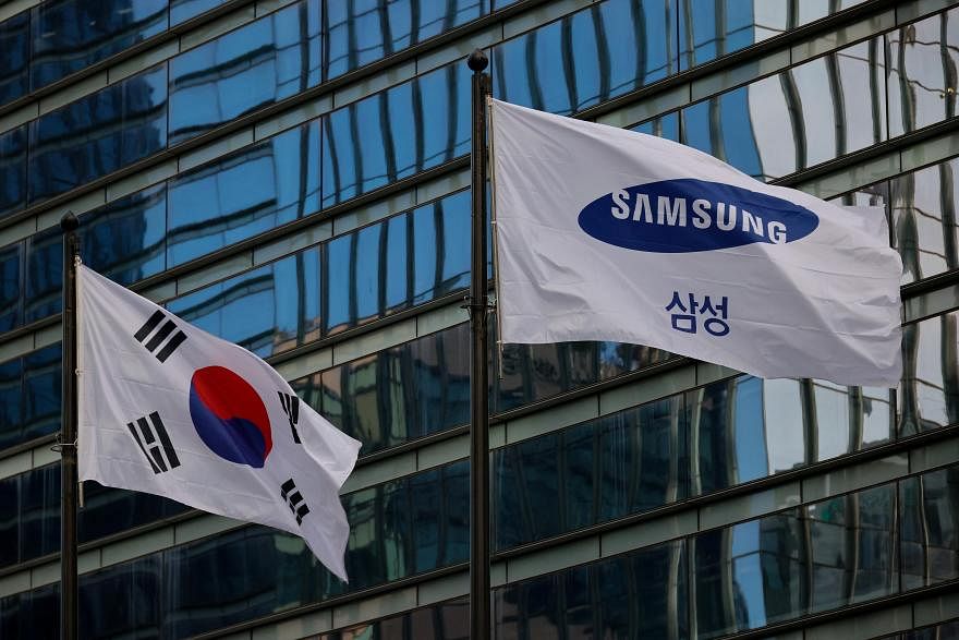
Korea CHips Act 2024.jpg

THE United States plans to award more than US$6 billion to Samsung Electronics, helping the chipmaker expand beyond a project in Texas it has already announced, according to sources familiar with the matter.


The money from the 2022 Chips and Science Act would be one of several major awards that the Commerce Department is expected to announce in the coming weeks, including a grant of more than US$5 billion to Samsung’s Asian rival, Taiwan Semiconductor Manufacturing Company (TSMC), sources familiar with the plans said earlier. The sources spoke on condition of anonymity in advance of the official announcements.

The federal funding for Samsung, South Korea’s leading chipmaker, would come alongside significant additional US investment by the firm, the sources said. In 2021, the company announced a US$17 billion project in Taylor, Texas, near an existing Samsung plant in Austin. It is not yet clear where the additional investment would be located.

The pending announcement only represents a preliminary agreement that could still change, and no final decision has been made. Samsung and the Commerce Department declined to comment, while the White House did not respond to a request for comment.

The Chips Act set aside US$39 billion in direct grants – plus loans and loan guarantees valued at US$75 billion – to persuade the world’s top semiconductor companies to make chips on American soil after decades of production abroad.

The Commerce Department earlier announced three Chips Act grants to producers of older-generation semiconductors. Officials have been negotiating for months with makers of cutting-edge chips that will fuel the artificial intelligence boom, and have set aside about US$28 billion for those advanced projects, Commerce Secretary Gina Raimondo has said.
 

Seems pretty obvious that once mod 1 gets built they plan to do a mod 2. Definitely a more relaxed pace than TSMC or intel Arizona where they are doing two fabs at the same time. I also think the way Samsung is doing their utilities here is very interesting (just two long lone lines flanking the fab). I wonder if the site is legally allowed to be larger the 2 fabs? since the property they have is really big, and it is not hard to imagine another 2 fabs to the left or right with a skybridge connecting the cleanrooms. But maybe 2 is all they or the Texan government want. After all that is what happened with Samsung Austin. If that is the case though it seems wasteful to not do it like TSMC AZ (6) or intel ohio (8) to have the optionality for at least 4 fabs.

Another interesting idea. Maybe Samsung will do some memory in the US again? Their original Texas fab was a small flash fab before getting converted to 65nm logic. Maybe Taylor 2 can be a dram and or flash fab to compete with Micron for USG grants? Only problem I see with that is one mod that is only 1 cleanroom floor would be subscale vs those Godzilla sized fabs in Korea or Micron NY when/if it is fully built
Phase 1 or T1 is the first building, Phase 2 is part of the initial construction with infrastructure & possibly a shell building. The site is extendable up to 10 fabs, and Samsung submitted applications to the state of Texas for up to 11 facilities and the related tax exemptions. This is almost certainly not limited to 1, or even 2 fabs at the Taylor site.
 
Phase 1 or T1 is the first building, Phase 2 is part of the initial construction with infrastructure & possibly a shell building. The site is extendable up to 10 fabs, and Samsung submitted applications to the state of Texas for up to 11 facilities and the related tax exemptions. This is almost certainly not limited to 1, or even 2 fabs at the Taylor site.
Is there a copy of the proposal floating around? I tried looking a while ago and this was the best thing I found:
1710515951784.png

1710516021211.png


Or maybe the maximum site size information is in their earnings statements?
 
Back
Top