Array
(
    [content] => 
    [params] => Array
        (
            [0] => /forum/index.php?threads/intels-foundry-business-discloses-a-7b-operating-loss.19951/page-4
        )

    [addOns] => Array
        (
            [DL6/MLTP] => 13
            [Hampel/TimeZoneDebug] => 1000070
            [SV/ChangePostDate] => 2010200
            [SemiWiki/Newsletter] => 1000010
            [SemiWiki/WPMenu] => 1000010
            [SemiWiki/XPressExtend] => 1000010
            [ThemeHouse/XLink] => 1000970
            [ThemeHouse/XPress] => 1010570
            [XF] => 2021370
            [XFI] => 1050270
        )

    [wordpress] => /var/www/html
)

Intel's Foundry Business discloses a $7B operating loss

Gaming PCs are not a "relatively small market". Nvidia sold just under $3B of GeForce GPUs in 2023, impressive considering that the majority of the gaming market is now integrated graphics. While revenue-wise that's only 25% of Nvidia's data center GPU sales, the entire PC gaming hardware market is estimated at over $50B with a 12.9% CAGR. AI GPUs are Nvidia's future, but Intel isn't on that track (yet, I hope for their sake). Like I said, I've never thought Intel's client-first strategy was a good thing for data center silicon, but it still looks like Intel's strategy.

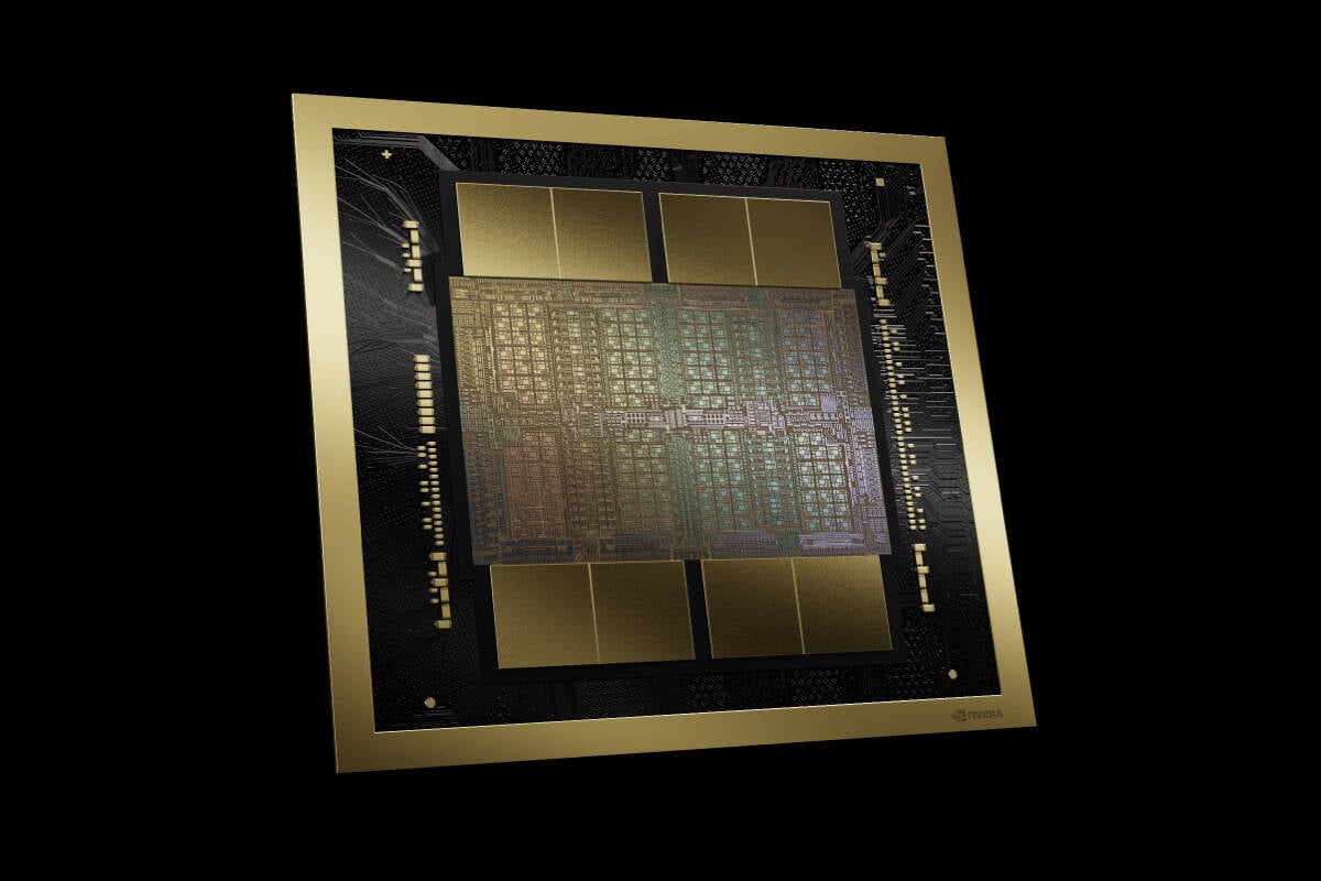
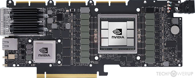
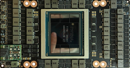
I said that gaming PCs (CPUs) are a relatively small and shrinking part of the total leading-edge silicon market; yes they're still growing -- at least, for the time being -- but the total market is predicted to grow faster, and the vast majority of this growth is predicted to be in AI, especially engines at the hyperscalars (about 50%/year CAGR) but also GPUs at the endpoints. By the time all this gets into its stride in 18A/N2, this market will be bigger than gaming PCs, even including the GPUs inside these, and much bigger than the CPUs where single-core speed is headlined (but increasingly less relevant).

That's what TSMC say, they're building their business in the next few years based on this, so I tend to believe them ;-)

My point is that maximum single-core (or even multi-core) clock rate (6GHz!!!) so beloved by gamers (and Intel...) is becoming less and less important, and density (cost) and power efficiency (heat) are becoming more and more important -- at least, as far as the biggest markets for the most advanced nodes are concerned.

So that's where the process should be targeted if you want to give (most big) customers what they're looking for -- and it's clearly what TSMC are doing, because these are already their customers.

In contrast Intel is coming from an IDM background where the biggest customer was themselves (x86 CPUs) and their headline #1 target was clock rate, with power consumption/density/cost coming second -- and their processes (including 18A) still seem to be targeted at this market.
 
Last edited:
All true -- but you're still looking at today's HPC, which is not where the massive use of these processes is predicted to be... ;-)

Nvidia standalone GPUs are trying to push the biggest performance possible out of a given-sized piece of silicon, often reticle sized in their biggest parts -- and as a consequence power is anything up to 500W or so. For Blackwell the most power-efficient part (in flops/W) is not the biggest one -- which dissipates 1000W! -- but the smaller one (presumably run at slightly lower clock rate and voltage), with 10%-20% lower power per flop. Which is equivalent to maybe a half-node...


Remember these are in N4P, so if you go to N2 (2 node jump) a reticle-size chip would give perhaps double the throughput but also dissipate maybe 50% more power -- and 1500W per chip is getting ridiculously difficult to deal with. What is more likely is that they'll back off voltage and clock speed to sacrifice some throughput but lower power consumption my rather more. But then when you look at what can be fitted into a rack (and cooled) the picture changes again because interconnect comes into it more...

I've spent a lot of time doing exactly this kind of PPA analysis (based on real signal processing circuits, not idealised gates) for N5/N4/N3, and unless absolute maximum throughput regardless of power is the #1 criterion (which it might be for one GPU in a PC) you normally find that when going up a node the voltage drops a little bit, the clock rate doesn't go up much (if at all) but power per gate/flop drops significantly -- throughput per chip goes up because there are more gates, power per flop drops faster then if you stayed at the same voltage, but it still gets harder to cool... :-(
Excuse my ignorance Ian, but I guess a few questions. The way NVIDIA makes their new product more valuable than the old one is improving the flops/$, yes? If so then I assume we would agree that the best way to increase the number of flops/$ is to increase energy efficiency because over the lifetime of the DC power consumption is one of the main costs.

Looking at the flagship A100s and H100s:
NVIDIA ratcheted up the base clocks 100% and turbo clocks 38%.
TDP went up 2.3X
SM and Tensor core counts both went up 22%

Power consumption went up alot on a per SM basis, and clocks also increased significantly too (faster than the SM count). Yet H100 is significantly more efficient than A100. Yes I know the architecture got better and bandwidth is 65% higher, but I feel like these statistics don't line up with only using the superior N4 HPC process to shift their freq/power curve down. They must have used N4 to move some amount to shift the curve some amount to the right. I have to assume that the clock speed scaling will slow down, because the difference is insane (to the point I had to check elsewhere because it seemed way to high to be real I couldn't find the base but the boost does seem to be right). Why is this the case? If lowering power at iso performance is always the best way to maximize work done/energy consumed, why does NVIDIA's best not shift their new power curve straight down?

If you look at the power/performance curves from one node to the next, for power-critical applications you find that somewhere not far off the same performance (clock rate) is the best choice -- you drop the voltage a bit (maybe a few 10s of mV), keep the same clock rate, and save power/flop (maybe 25% per node nowadays?). For the same size chip you then get more throughput (e.g. +50%) because the density is higher (e.g. 50% more parallel circuits), but the overall power still goes up (e.g. 20%) for the same size chip.

Trying to push clock rates up is a loser, partly because the metal is getting thinner and more resistive so interconnect delays are getting longer and longer compared to gate delays, and partly because power efficiency almost always drops -- assuming you can fit more slower circuits on the silicon, which may not be possible if you've run out of silicon... :-(

We've been through this process for N7/N5/N4/N3 and ended up using similar clock rates, but saving a lot of power for the same function -- however you then cram more and more function onto the chip each time which pushes the power back up again... ;-)

OTOH we're not in the Nvidia position of maxing out reticle sizes and needing to get as much function as possible out of a 700mm2 chip, which can then force them to push them more up the power curve and down the efficiency curve.

As usual there's no simple answer to a complex problem, the optimum solution is different for each device depending on priorities, activity factor, latency and so on -- you need to figure out what is best for your particular device, and it may well be different to what is best for somebody else's. But what is clear is the the gains (power, speed, density, cost) from going to the next node are continually getting smaller and the cost of doing this is continually increasing... :-(
 
Bernstein analysts said on Friday that their primary takeaway from Intel’s (INTC) foundry segmentation event was “No real reason to be here until 2030.”

The chipmaker’s shares dropped by roughly 8% since the company's disclosure of its semiconductor manufacturing arm's financial performance in its semiconductor manufacturing business, also called the foundry segment.

Specifically, the foundry posted a $7 billion operating loss in 2023, against revenues of $18.9 billion. This loss marks an increase from the $5.2 billion loss recorded in 2022, with sales previously at $27.5 billion.

“After all, the fact that foundry economics have been awful is not (or should not have been) a huge surprise; in fact the company directly suggested this back in June,” analysts said.

“That being said, the idea that things are still getting worse in 2024 might have been taken somewhat poorly; if anything, the idea that a -37% operating margin and $7B loss do not yet represent a trough is somewhat breathtaking especially given all the cost cuts the company was supposedly implementing last year.”

Bernstein acknowledges the potential for improvement in Intel (NASDAQ:INTC)'s foundry business, noting its significant loss last year and the optimistic forecast for a 25-30% operating margin by 2030.

However, analysts expressed caution, suggesting that it may be a long ride for INTC “even if one is fully signed up to the (seemingly aggressive) targets.”

They highlighted that achieving break-even may not be feasible until after 2027, and the ambitious 2030 targets remain speculative, hinging on optimal progress, “which remains a wide
open debate.”

Just to re-iterate couple points. This P&L is not just due to 2022 downturn or to skipping EUV or to too many expedites. The issue is that that the process could be as inefficient as needed to get the product out. So that is what was done. It works great as a IDM. its is not good as a foundry. On the positive side, Intel Product Co will get major cost improvements from using TSMC in 2024 and 2025.

The timeline for improvement and the perception that even 18A is not really leading was a shock to most people. When people realize that 18A will not be significant volume for many years it might become a bigger problem. Lets see how Intel 3 and Intel 20A works out since those should be ramping in next 9 months and the rumors are starting to swirl based on customer updates.
one input, the tool re-used rate from n node to n+1/n+2 nodes could be more than 80% or even up to 95%, which is good sign for new tool/new fab investment.
 
This is an interesting slide:
- Performance/watt - I agree with their ratings.
- Density - I don't agree with, TSMC is way ahead of 18A, maybe Intel could catch up at 14A but it would take a huge jump.
- Wafer cost - surprisingly, I was just looking at wafer cost and through 18A I think they are correct, I need to look at 14A some more, maybe it will be a plus if they bet right on High NA and TSMC bet wrong.
- I don't really have an opinion on the bottom 3 lines.

What TSMC node are you comparing it to? N3 or N2? According to an Intel source it is compared to TSMC N3.
 
Back
Top