
Still Intel expects 18A be a big and profitable node. It should be REALLY great then...I kinda see why they needed to introduce PowerVIA(BSPDN) earlier than competitors...I have actual numbers for 18A pitches, I can't publish them but I can say that 18A high density cell transistors per mm2 are slightly higher than TSMC 5nm but lower than TSMC 3nm. To even catch up to TSMC 2nm, Intel 14A would need a big density jump and this is during a time when density jumps are getting harder.
Array
(
    [content] =>
    [params] => Array
        (
            [0] => /forum/index.php?threads/intels-foundry-business-discloses-a-7b-operating-loss.19951/page-3
        )

    [addOns] => Array
        (
            [DL6/MLTP] => 13
            [Hampel/TimeZoneDebug] => 1000070
            [SV/ChangePostDate] => 2010200
            [SemiWiki/Newsletter] => 1000010
            [SemiWiki/WPMenu] => 1000010
            [SemiWiki/XPressExtend] => 1000010
            [ThemeHouse/XLink] => 1000970
            [ThemeHouse/XPress] => 1010570
            [XF] => 2021370
            [XFI] => 1050270
        )

    [wordpress] => /var/www/html
)
Guests have limited access.
Join our community today!
Join our community today!
You are currently viewing SemiWiki as a guest which gives you limited access to the site. To view blog comments and experience other SemiWiki features you must be a registered member. Registration is fast, simple, and absolutely free so please, join our community today!
You are using an out of date browser. It may not display this or other websites correctly.
You should upgrade or use an alternative browser.
You should upgrade or use an alternative browser.
Intel's Foundry Business discloses a $7B operating loss
- Thread starter blueone
- Start date
For 18A, the target segment is HPC (noteably ‘not mobile’). Is it possible that the density estimate vs competition is correct for that segment? High performance libraries for comparison instead of high density?This is the most interesting slide. The dash means Intel is behind, the squiggles means Intel is comparable and plus means ahead. They don't say who the comparison is with but clearly it is TSMC. They key here is the Target Segment, so this is in terms of HPC. As far as performance goes I agree with this graphic but not performance per watt. I have a problem with wafer cost especially when yield is involved. I also do not agree with the 18A density comparison, if we are talking about TSMC. Samsung 2nm maybe, TSMC N2 no. EDA ease of use I can agree with since Intel is a big EDA customer but TSMC has the biggest EDA/IP ecosystem. Packaging is still a wait and see for me. Intel and Samsung are not doing packaging HVM for foundry customers as of yet in comparison to TSMC. On paper maybe but foundry HVM is a different deal altogether.
View attachment 1809
Last edited:
When you sayWhen comparing wafer costs there are two components, one is process cost and the other is fab cost. Intel 10/7 processes are very expensive processes compared to TSMC 7nm even if run in the same fab. Intel fabs are generally in higher cost countries plus Intel has some Intel specific cost disadvantages. The net of this is Intel 10/7 cost is similar to TSMC selling price. The interesting thing is 18A as a process run in the same fabs as TSMC 2nm is actually a lower cost process, 18A is lower density and needs less EUV layers. Intel still has Fab cost issues but the cost to run 18A in Arizona Fab 52 versus TSMC 2nm in Fab 20-P1 is well below TSMC selling price. It is lower density but better raw performance so it depends on your needs.
Also, for the record all my wafer costs are calculated using the commercial models I sell that calibrate to published financials and inputs from a huge customer base. When I compare companies I always us the same depreciation rates to make it consistent.
I assume you mean it's lower cost *per wafer* (in the same fab)?18A as a process run in the same fabs as TSMC 2nm is actually a lower cost process, 18A is lower density and needs less EUV layers
Given the density difference (IIRC this is quite large?) this could mean the cost per chip (same function) is similar or maybe higher in 18A than TSMC 2nm -- and that's ignoring yield and fab utilization (and running cost), where we know TSMC has had the advantage for many years, which will further skew the cost in their favour and against Intel.
Last edited:
Yes, but even the TSMC HPC libraries are denser than Intel -- as Scotten said above Intel use more relaxed design rules and fewer EUV layers (and presumably fewer DP EUV layers too...) so 18A is just plain inherently less dense.For 18A, the target segment is HPC (noteably ‘not mobile’). Is it possible that the density estimate vs competition is correct for that segment? High performance libraries for comparison instead of high density?
OTOH it may have higher ultimate performance, if you can afford the resulting power penalty and larger die size/cost, so it may win for some products (e.g. Intel CPUs). But the over-riding drives for most products nowadays are cost/size for a given die/function and power efficiency for large/multicore dies and N2 is likely to win on both counts, not absolute maximum clock rate (at high voltage/power) where 18A could well win against N2.
Last edited:
tooLongInEDA
Moderator
There appears to be some concensus here than N2 is denser than 18A. But is that by enough to offset the increased process complexity cost (more EUV layers) and maintain the overall cost lead ?Yes, but even the TSMC HPC libraries are denser than Intel -- as Scotten said above Intel use more relaxed design rules and fewer EUV layers (and presumably fewer DP EUV layers too...) so 18A is just plain inherently less dense.
OTOH it may have higher ultimate performance, if you can afford the resulting power penalty and larger die size/cost, so it may win for some products (e.g. Intel CPUs). But the over-riding drives for most products nowadays are cost/size for a given die/function and power efficiency for large/multicore dies and N2 is likely to win on both counts, not absolute maximum clock rate (at high voltage/power) where 18A could well win against N2.
More generally, the implication is that Intel's 18A is targetting a market segement of the foundry business (HPC) and not the entire market TAM. And this may indeed be a sensible strategy. But does that square with their stated aim to be the #2 foundry ? Are they still missing processes and technologies to serve a large enough market ?
Mooredaddy
Well-known member
My question is this. IFS is losing money hand over fist. And Intel products are losing market share to AMD and bespoke big tech ARM designs. Intel products is the only profitable segment, and it is under assault from all sides. How does intel expect to fund the unprofitable fab business for the next couple years without taking increasing large amounts of debt, mortgaging the future with their “smart capital system” where they give up 49% profits of a fab up to Brookfield. Government funding is not going to be there to permanently backstop these losses. Pat and the boards argument seems to be that their products division will magically gain back share all the while IFS is magically profitable enough through sheer utilization rates via outside designs to be profitable. Essentially everything has to go right, no? And not just kind of right, but spectacularly right. It seems clear from these technical specs that 18A won’t be the magical node to send Intel back to the golden years that many hope it will be. Intel is going to have to eat costs in IFS to convince people to switch and made it worth their while, all while making a superior process - of which that seems to very much be in doubt now. I understand density is not the be all and end all but I find it hard to believe that when N2 with its higher density gets BPD it will be a easy sell to move to 14A etc.There appears to be some concensus here than N2 is denser than 18A. But is that by enough to offset the increased process complexity cost (more EUV layers) and maintain the overall cost lead ?
More generally, the implication is that Intel's 18A is targetting a market segement of the foundry business (HPC) and not the entire market TAM. And this may indeed be a sensible strategy. But does that square with their stated aim to be the #2 foundry ? Are they still missing processes and technologies to serve a large enough market ?
Last edited:
Excellent questions, which leads to another question. Could IFS win a high-volume mobile device customer, larger than their own internal CPU customers, in the 18A timeframe? I doubt it. So, business-wise, it looks like optimizing for performance over density was the best decision. Being the #2 foundry seems like an objective farther out than 18A too.More generally, the implication is that Intel's 18A is targetting a market segement of the foundry business (HPC) and not the entire market TAM. And this may indeed be a sensible strategy. But does that square with their stated aim to be the #2 foundry ? Are they still missing processes and technologies to serve a large enough market ?
30% of Intels wafers used are from TSMC in 2024. Meteor lake, Lunar lake, Arrow Lake, Panther lake 70% of the Silicon is TSMC with backup plans that can take that higher.
When Pat talks about TSMC usage I believe he is talking about design and not manufacturing or actual parts shipped. In my opinion 2025 will be a big year for TSMC N3 revenue based on Intel parts, not 2024. From what I hear Intel should be TSMC's #2 customer in 2024, 2025, 2026. Hopefully Intel can replace TSMC N3 with 18A. Intel will not be using TSMC N2 from what I hear but N3 supporting chiplets can be used for a long time.
Agreed. This is what's called "betting the company". And it is a risky bet.Pat and the boards argument seems to be that their products division will magically gain back share all the whole IFS is magically profitable enough through sheer utilization rates via outside designs to be profitable. Essentially everything has to go right, no? And not just kind of right, but spectacularly right. It seems clear from these technical specs that 18A won’t be the magical node to send Intel back to the golden years that many hope it will be. Intel is going to have to eat costs in IFS to convince people to switch and made it worth their while, all while making a superior process - of which that seems to very much be in doubt now. I understand density is not the be all and end all but I find it hard to believe that when N2 with its higher density gets BPD it will be a easy sell to move to 14A etc.
Where is the Intel 20A in this slide? Did Intel decide to kill/skip it?
With the introduction of 14A and its technical superiority, does that mean Intel push the year of gaining leadership position over TSMC further down to a future date?
Pat was talking about IFS which does not offer Intel 4 or 20A.
The problem Intel may have is that they still seem to mentally think "HPC=Highest GHz clock rate" because this is the marketing point for their x86 CPUs -- fastest single-core boost frequency to make a headline against AMD, for example.There appears to be some concensus here than N2 is denser than 18A. But is that by enough to offset the increased process complexity cost (more EUV layers) and maintain the overall cost lead ?
More generally, the implication is that Intel's 18A is targetting a market segement of the foundry business (HPC) and not the entire market TAM. And this may indeed be a sensible strategy. But does that square with their stated aim to be the #2 foundry ? Are they still missing processes and technologies to serve a large enough market ?
This is less and less important even for desktop/laptop CPUs where running the cores flat out at highest voltage might give the highest benchmark score but at a disproportionate cost in power/energy consumption.
It's certainly becoming less and less critical for massively-parallel HPC applications where energy efficiency -- pJ/flop -- is becoming the key point, because a chip that dissipates more than 1000W (including GPU and AI chips) to give double the throughput of a 250W chip is a bad deal, so these all tend to run at lower clock rates and voltages (e.g. lower gate depth 2GHz 0.8V) not high clock rates and voltages (e.g. highly pipelined 5GHz at >1V).
This is being driven more and more as processes shrink because power density in W/mm2 keeps rising as gates shrink faster than power consumption falls.
So it may well be the case that Intel is optimising 18A for the wrong "old-school-HPC" target (faster, less dense, less efiicient) not the "new-wave-HPC" target (slower, denser, more efficient) -- which is where TSMC has been the winner in the past.
Except "perfomance" in HPC nowadays (and especially in future) is more likely to mean "most efficient/dense" not "highest clock rate", especially in what is predicted to be the dominant market driver which is AI not traditional CPUs.Excellent questions, which leads to another question. Could IFS win a high-volume mobile device customer, larger than their own internal CPU customers, in the 18A timeframe? I doubt it. So, business-wise, it looks like optimizing for performance over density was the best decision. Being the #2 foundry seems like an objective farther out than 18A too.
For gaming PCs, which remains a huge global market, highest single thread clock speed is still best for many (most, I think) games. More importantly, serious gamers seem to think the highest clock speed is the best and make purchase decisions that way, regardless of what the reality might be for an individual game. Intel may have its problems, but they did successfully execute on over-clocking support. At heart, Intel still appears to think "client first", which always frustrated me as a data center sort of guy.Except "perfomance" in HPC nowadays (and especially in future) is more likely to mean "most efficient/dense" not "highest clock rate", especially in what is predicted to be the dominant market driver which is AI not traditional CPUs.
Regardless of what gamers think, gaming PCs (CPUs) are a relatively small and shrinking part of the total leading-edge silicon market -- the dominant market driver in these timescales (18A vs. N2) will be HPC at the hyperscalars, more specifically AI which will be >10x bigger than gaming CPUs -- even in these there's a lot more silicon in the GPU than the CPU. For this "future-HPC" market nobody cares one jot about highest clock speed, power efficiency and total throughput for massively parallel cores are king.For gaming PCs, which remains a huge global market, highest single thread clock speed is still best for many (most, I think) games. More importantly, serious gamers seem to think the highest clock speed is the best and make purchase decisions that way, regardless of what the reality might be for an individual game. Intel may have its problems, but they did successfully execute on over-clocking support. At heart, Intel still appears to think "client first", which always frustrated me as a data center sort of guy.
See TSMCs recent "state of the industry" presentation... ;-)
Last edited:
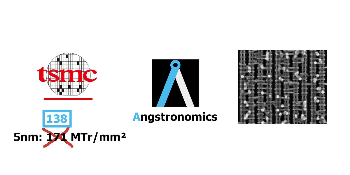
According to an Angstronomics article (linked below) Intel 4 is denser than TSMC N5:I have actual numbers for 18A pitches, I can't publish them but I can say that 18A high density cell transistors per mm2 are slightly higher than TSMC 5nm but lower than TSMC 3nm. To even catch up to TSMC 2nm, Intel 14A would need a big density jump and this is during a time when density jumps are getting harder.
So, if 18A is only slightly more dense that N5, then it must be less dense, or equally dense as Intel 4. Can this be true?H280g57 gives a logic density of 92.3 MTr/mm² for 3-fin N5.... while Intel 4’s sole 3-fin library (H240g50) has a density of 122.8 MTr/mm².

This is a far too simplistic way of looking at it IMO. TSMC mobile process and HPC are not the same. A phone SOC needs ultra low leakage to maximize battery life and they pay for that with higher active power consumption. HPC wants the best performance in a given power envelop. Intel client CPUs live in their own little world of just highest performance at all other costs. If you look at a Xeon on the other hand those cores run at extremely low voltages because as you said it lets you slap down more cores in your TDP and get a bigger performance boost than only scaling freq. As for your comment of "slow, dense, more efficient.", I would argue there is nothing "new" about it. This was the driving factor for computers to move to transistors and later ICs instead of tubes, this is why amd/intel integrated more functionality (IMC, graphics, IO controllers) onto their CPUs, etc etc.The problem Intel may have is that they still seem to mentally think "HPC=Highest GHz clock rate" because this is the marketing point for their x86 CPUs -- fastest single-core boost frequency to make a headline against AMD, for example.
This is less and less important even for desktop/laptop CPUs where running the cores flat out at highest voltage might give the highest benchmark score but at a disproportionate cost in power/energy consumption.
It's certainly becoming less and less critical for massively-parallel HPC applications where energy efficiency -- pJ/flop -- is becoming the key point, because a chip that dissipates more than 1000W (including GPU and AI chips) to give double the throughput of a 250W chip is a bad deal, so these all tend to run at lower clock rates and voltages (e.g. lower gate depth 2GHz 0.8V) not high clock rates and voltages (e.g. highly pipelined 5GHz at >1V).
This is being driven more and more as processes shrink because power density in W/mm2 keeps rising as gates shrink faster than power consumption falls.
So it may well be the case that Intel is optimising 18A for the wrong "old-school-HPC" target (faster, less dense, less efiicient) not the "new-wave-HPC" target (slower, denser, more efficient) -- which is where TSMC has been the winner in the past.
Taking a look at the current poster boy of HPC, NVIDIA, they don't practice "slow" for their Xtors. If HPC was only a function of lowering power NVIDIA would operate at Vmin and lower their freq below their fmax @Vmin to minimize active power. Yet they don't do this, and instead they do push freq pretty hard for a GPU, taking care to not have the freq inc to be greater than the resulting loss in core count. It seems like they find a voltage and core count config that gives the best performance in a power envelop and then cranks freq as fast as they can get it at that voltage. For those smaller GPU dies that means higher freq and the bigger dies spend more of their power budget on cores lowering the voltage they have to operate with.
That is on a 3 fin to 3 fin logic cell basis. TSMC's N5 2 fin HD cell is 210h and is a bit denser than intel 4 HP library. I don't like the undercurrent of N5 being not as good as promised that permeates this article either. N5 was and still is a very compelling process. While TSMC was detail light with their pre-launch communications about N5, everything they said would be there is there.According to an Angstronomics article (linked below) Intel 4 is denser than TSMC N5:
So, if 18A is slightly more dense that N5, then it must be less dense, or equally dense as Intel 4. Can this be true?
Last edited:
According to an Angstronomics article (linked below) Intel 4 is denser than TSMC N5:
So, if 18A is only slightly more dense that N5, then it must be less dense, or equally dense as Intel 4. Can this be true?
Intel Reports Q2 2023 Financial Results with Strong Guidance!
Intel Q2 Non-GAAP EPS of $0.13 beats by $0.16. Revenue of $12.9B (-15.7% Y/Y) beats by $760M but down 15% YoY Forecasting third-quarter 2023 revenue of approximately $12.9 billion to $13.9 billion vs $13.28B consensus Expecting third-quarter EPS attributable to Intel of $0.04 Non-GAAP EPS...
semiwiki.com
Gaming PCs are not a "relatively small market". Nvidia sold just under $3B of GeForce GPUs in 2023, impressive considering that the majority of the gaming market is now integrated graphics. While revenue-wise that's only 25% of Nvidia's data center GPU sales, the entire PC gaming hardware market is estimated at over $50B with a 12.9% CAGR. AI GPUs are Nvidia's future, but Intel isn't on that track (yet, I hope for their sake). Like I said, I've never thought Intel's client-first strategy was a good thing for data center silicon, but it still looks like Intel's strategy.Regardless of what gamers think, gaming PCs (CPUs) are a relatively small and shrinking part of the total leading-edge silicon market -- the dominant market driver in these timescales (18A vs. N2) will be HPC at the hyperscalars, more specifically AI which will be >10x bigger than gaming CPUs -- even in these there's a lot more silicon in the GPU than the CPU. For this "future-HPC" market nobody cares one jot about highest clock speed, power efficiency and total throughput for massively parallel cores are king.
See TSMCs recent "state of the industry" presentation... ;-)
Gaming PC Market Size, Share And Trends Report, 2030
The global gaming PC market size was valued at USD 50.23 billion in 2022 and is expected to grow at a CAGR of 12.9% from 2023 to 2030
but that's not fair - you can't compare a HD library with a HP library. It'd be interesting to compare N5 with Intel 3 HD library, but I assume those tech details are not know.That is on a 3 fin to 3 fin logic cell basis. TSMC's N5 2 fin HD cell is 210h and is a bit denser than intel 4 HP library. I don't like the undercurrent of N5 being not as good as promised that permeates this article either. N5 was and still is a very compelling process. While TSMC was detail light with their pre-launch communications about N5, everything they said would be there is there.
All true -- but you're still looking at today's HPC, which is not where the massive use of these processes is predicted to be... ;-)This is a far too simplistic way of looking at it IMO. TSMC mobile process and HPC are not the same. A phone SOC needs ultra low leakage to maximize battery life and they pay for that with higher active power consumption. HPC wants the best performance in a given power envelop. Intel client CPUs live in their own little world of just highest performance at all other costs. If you look at a Xeon on the other hand those cores run at extremely low voltages because as you said it lets you slap down more cores in your TDP and get a bigger performance boost than only scaling freq. As for your comment of "slow, dense, more efficient.", I would argue there is nothing "new" about it. This was the driving factor for computers to move to transistors and later ICs instead of tubes, this is why amd/intel integrated more functionality (IMC, graphics, IO controllers) onto their CPUs, etc etc.
Taking a look at the current poster boy of HPC, NVIDIA, they don't practice "slow" for their Xtors. If HPC was only a function of lowering power NVIDIA would operate at Vmin and lower their freq below their fmax @Vmin to minimize active power. Yet they don't do this, and instead they do push freq pretty hard for a GPU, taking care to not have the freq inc to be greater than the resulting loss in core count. It seems like they find a voltage and core count config that gives the best performance in a power envelop and then cranks freq as fast as they can get it at that voltage. For those smaller GPU dies that means higher freq and the bigger dies spend more of their power budget on cores lowering the voltage they have to operate with.
That is on a 3 fin to 3 fin logic cell basis. TSMC's N5 2 fin cell is 210h if memory serves and is a bit denser than intel 4 HP library.
Nvidia standalone GPUs are trying to push the biggest performance possible out of a given-sized piece of silicon, often reticle sized in their biggest parts -- and as a consequence power is anything up to 500W or so. For Blackwell the most power-efficient part (in flops/W) is not the biggest one -- which dissipates 1000W! -- but the smaller one (presumably run at slightly lower clock rate and voltage), with 10%-20% lower power per flop. Which is equivalent to maybe a half-node...
What Nvidia's Blackwell efficiency gains mean for DC owners
Air cooling's diminishing returns on full display with Nv's B-series silicon
 www.theregister.com
Remember these are in N4P, so if you go to N2 (2 node jump) a reticle-size chip would give perhaps double the throughput but also dissipate maybe 50% more power -- and 1500W per chip is getting ridiculously difficult to deal with. What is more likely is that they'll back off voltage and clock speed to sacrifice some throughput but lower power consumption my rather more. But then when you look at what can be fitted into a rack (and cooled) the picture changes again because interconnect comes into it more...
I've spent a lot of time doing exactly this kind of PPA analysis (based on real signal processing circuits, not idealised gates) for N5/N4/N3, and unless absolute maximum throughput regardless of power is the #1 criterion (which it might be for one GPU in a PC) you normally find that when going up a node the voltage drops a little bit, the clock rate doesn't go up much (if at all) but power per gate/flop drops significantly -- throughput per chip goes up because there are more gates, power per flop drops faster then if you stayed at the same voltage, but it still gets harder to cool... :-(