Array
(
    [content] => 
    [params] => Array
        (
            [0] => /forum/index.php?threads/how-is-backside-power-really-done.19399/
        )

    [addOns] => Array
        (
            [DL6/MLTP] => 13
            [Hampel/TimeZoneDebug] => 1000070
            [SV/ChangePostDate] => 2010200
            [SemiWiki/Newsletter] => 1000010
            [SemiWiki/WPMenu] => 1000010
            [SemiWiki/XPressExtend] => 1000010
            [ThemeHouse/XLink] => 1000970
            [ThemeHouse/XPress] => 1010570
            [XF] => 2021370
            [XFI] => 1050270
        )

    [wordpress] => /var/www/html
)

How is backside power really done?

mozartct

Active member
There are many threads about backside power but I am lost on a key point: when/how is the backside metal put in place?

Conventionally, a finished wafer would be ground from the backside to expose vias.

In BP, it seems to be that the power lines are laid down first and the transistors are built on top. Is that really the case? I am not understanding how the wiring could survive diffusion, implant etc. Some of these steps are very energetic and would presumably ruined the underlying metal (by allowing barrier films and metal films for example). Additionally, what kind of epi structure do you get by etching deep trenches, filling them with metal and then laying down oxide and then epi on top?

I must be missing something.
 
There are many threads about backside power but I am lost on a key point: when/how is the backside metal put in place?

Conventionally, a finished wafer would be ground from the backside to expose vias.

In BP, it seems to be that the power lines are laid down first and the transistors are built on top. Is that really the case? I am not understanding how the wiring could survive diffusion, implant etc. Some of these steps are very energetic and would presumably ruined the underlying metal (by allowing barrier films and metal films for example).
While unsatisfying you will have to wait a bit longer for ARL when everyone and their mother starts doing 20A teardowns. But who knows maybe intel will be cool enough to go into a little bit of detail at the upcoming VLSI.
Additionally, what kind of epi structure do you get by etching deep trenches, filling them with metal and then laying down oxide and then epi on top?

I must be missing something.
Based on your statement it sounds like you are describing a BS-Contact. That is a different more advanced BSPD scheme than BPR or powerVIA. If I properly understand your meaning, an oxide insulation would defeat the purpose as the metal would connect to nothing. Also from my VERY limited understanding of epitaxial growth you'd need a seed which is always the exposed S/D Si. My understanding is the epi would not grow out of the oxide that you proposed to lay.
 
Last edited:
In BP, it seems to be that the power lines are laid down first and the transistors are built on top. Is that really the case? I am not understanding how the wiring could survive diffusion, implant etc. Some of these steps are very energetic and would presumably ruined the underlying metal (by allowing barrier films and metal films for example). Additionally, what kind of epi structure do you get by etching deep trenches, filling them with metal and then laying down oxide and then epi on top?
It seems likely that the nanovia contacts are created early, before the source/drain contacts. This might be similar to making contacts for buried power lines, so perhaps the recent IMEC papers on that give some clues on when and how that is done.

Superthinning for other products is generally accomplished with the aid of implanted oxygen, a few microns down, like creating an SOI wafer. Maybe they just start with an SOI wafer. The backside would be coarsely ground to maybe 50um or less, then they would switch to chemical etch which will stop at the oxygen. That should bring them close enough to planarize and start laying down the backside metal, meeting the nanovias at whatever level they penetrated.

Your point about thermal stress would still apply to the nanovias, so they would need to find compatible metal for that? Maybe tungsten with SiN barrier? Again, buried power would have had the same issues, so the IMEC papers may guide.
 
Last edited:
Let me clarify my thinking. In a basic TSV, I am etching a deep hole and filling it with either copper or W. As far as I know, this step is done AFTER the transistors are created. I finish my wafer, grind it, flip it and contact from the backside.

In BP, I would somehow create an entire "understructure" before starting to make the transistors and interconnects. ???

Unless we are taking about 2 wafers, one with the BP stuff and the other with the actual device. ???
 
Let me clarify my thinking. In a basic TSV, I am etching a deep hole and filling it with either copper or W. As far as I know, this step is done AFTER the transistors are created. I finish my wafer, grind it, flip it and contact from the backside.
That is a TSV last process. You can make it at other places too. Don't know what is best in which applications, but the point stands regardless.
1704738738385.png

1704738749964.png

In BP, I would somehow create an entire "understructure" before starting to make the transistors and interconnects. ???

Unless we are taking about 2 wafers, one with the BP stuff and the other with the actual device. ???
Oh... ok. What you are asking is pretty well documented. Attached are some well written articles on the topic. As for the BPR that is mentioned in the semiengineering article, the IMEC process requires a little bit of metal being embedded before the FEOL is formed. The actual backside metal layers then connect to this embedded metal. Based on the various whitepapers, every process I have seen forms the backside interconnect stack (ie BM0-BMx) after the FEOL and FS-BEOL (ie M0-Mx).

 
Last edited:
The real puzzle is how they maintain proper stress on the fins when so little silicon is under them to maintain the reference dimension. I can see that the base might be a micron or few, so yes it is stronger than the fins, but still below that you have relative mountains of copper and glass with their different expansions. There has to be some elegant engineering hidden in there to make that work.
 
"But with no power interconnects to get in the way, the lines in the M0 layer could be six nanometers further apart than they are today. That may not seem like much, but it means it takes less EUV effort to make them. For the process to be introduced next year and for its successor, “the cost savings we get from not scaling so aggressively more than offsets the additional cost from the backside power-delivery process,” Sell says."

Wow, that speaks volumes about EUV costs.
 
There are in fact many puzzles! I do my transistors and add TSVs, just like I would in flip. I bond a sacrificial wafer (so i can go through CMP later on), grind back to expose my vias. I then go through another 10-12 steps to build BP (combination of PVD, plating, CMP, CVD and etch). I would assume that the sacrificial wafer is removed, perhaps it's perforated glass and not silicon.

I get the improvement in pitch at M0 since the wider lines are no longer a factor, being on the backside.

On cost and yield, we shall see I guess. Comment from Tanj is dead on: how do you control stresses when there is nothing left of the original wafer?
 

Fwiw this ‘generic’ video from Intel 2 years ago uses certain phrasing that may help:

‘Using both sides of the wafer’ - indicating no second wafer

‘Nano TSVs’ - some kind of through the surface connection via ‘advanced packaging technology’ - it sounds like the chip is made as usual on the wafer (with signals only ‘on top of the chip’), and (after completion?) the nano TSVs are added via packaging later.

OP - this is my neophyte interpretation :)
 
In BP, it seems to be that the power lines are laid down first and the transistors are built on top. Is that really the case?
No, in a BP (semiconductor manufacturing) process, transistors are typically created first on a silicon wafer using various lithography and doping techniques. Subsequently, interconnect layers, including the metal wiring for power lines, are added above the transistors in the chip fabrication process.
 

Fwiw this ‘generic’ video from Intel 2 years ago uses certain phrasing that may help:

‘Using both sides of the wafer’ - indicating no second wafer

‘Nano TSVs’ - some kind of through the surface connection via ‘advanced packaging technology’ - it sounds like the chip is made as usual on the wafer (with signals only ‘on top of the chip’), and (after completion?) the nano TSVs are added via packaging later.

OP - this is my neophyte interpretation :)
There is a sacrificial wafer used on top to enable backside grinding and exposing the vias. That wafer is usually perforated glass. See TOK.
 
No, in a BP (semiconductor manufacturing) process, transistors are typically created first on a silicon wafer using various lithography and doping techniques. Subsequently, interconnect layers, including the metal wiring for power lines, are added above the transistors in the chip fabrication process.
Saimali, in a "conventional" wafer, the transistors are made and wiring is added on top. in BP (B = backside), power lines are added on the back of the wafer so underneath the transistors. So in the end, there is wiring beneath on above the active areas.
 
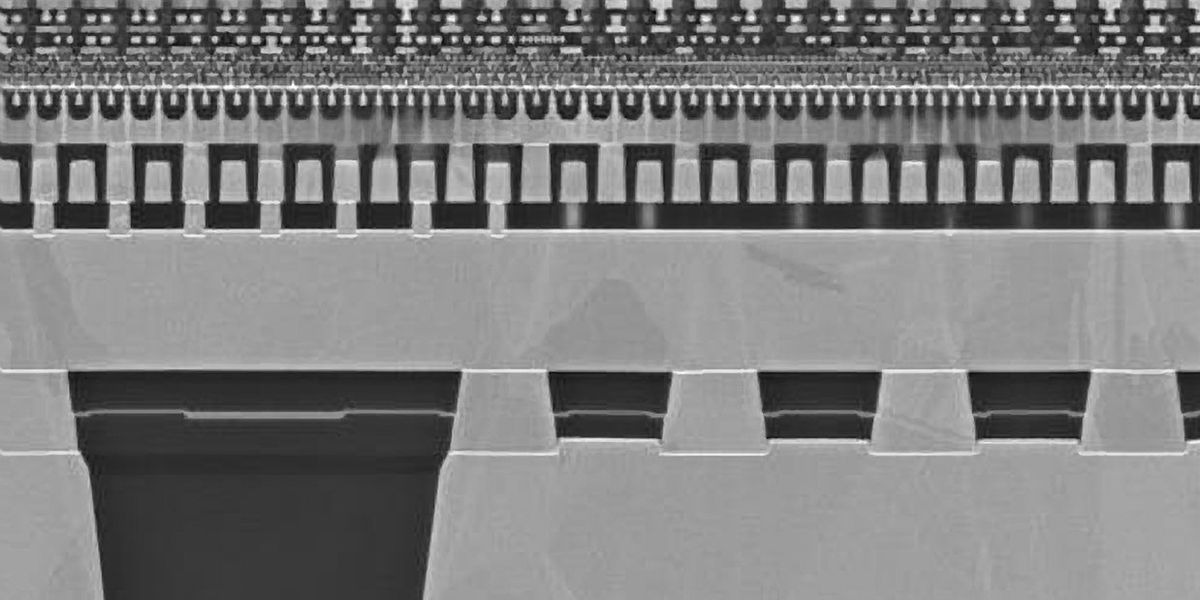
The Intel presentations imply they have gone for the "backside contact" approach which Cadence summarize as unsolved in that doc, though they also imply it might be the best if it could be done.
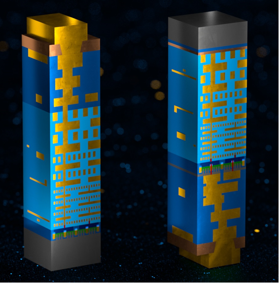
BS-contact is something they demod at IEDM. However intel has been pretty clear that is not what powerVIA is. This snippet from their marketing materiel presenting on their powerVIA findings at VLSI are probably as good as we will get without getting TEMs post launch or at a 20A whitepaper at VLSI.
1704923695249.png
 
BS-contact is something they demod at IEDM. However intel has been pretty clear that is not what powerVIA is. This snippet from their marketing materiel presenting on their powerVIA findings at VLSI are probably as good as we will get without getting TEMs post launch or at a 20A whitepaper at VLSI.
Those are the 3 things Synopsys describes, and that 3rd one is what Synopsys calls "backside contact".

That is a fascinating graphic. I wonder how accurate it is in conveying true scale, wiring pitch, etc. Probably it has been deliberately fuzzed.
 
Last edited:
Those are the 3 things Synopsys describes, and that 3rd one is what Synopsys calls "backside contact".
Not exactly. The Synopsys diagram and rest of industry seem to describe BS-Contacts as directly connecting to the EPI. I wish all of the IEDM papers were on IEEEexplore so I could snip some TEMs from the various papers, but alas not yet. When they do drop I would highly recommend taking a look. They are all nifty. Personally I am really excited to read the full TSMC/Samsung papers (rather than just the highlights that are widely available).

1704937244038.png

1704937308263.png
 
Last edited:
My understanding is the process is:
1) Transistor formation and front side interconnect formation on the front of the device wafer.
2) A carrier wafer is bonded to the front of the device wafer.
3) The wafer pair is flipped over and most of the device wafer is removed from the back.
4) Through silicon vias are formed through the device wafer from the back (this will depend on whose process it is, in some versions they could be created from the front and revealed during wafer thinning). I have discussed the Imec process with Buried Power Rail here: https://semiwiki.com/events/314464-imec-buried-power-rail-and-backside-power-delivery-at-vlsi/
5) Backside power layers are formed on the backside of the device wafer.

The carrier wafer is not removed and the signals as well as power have to come in through the backside. The backside power network is relatively sparse so there is plenty of room to bring in the signals.

The final device wafer is so thin that it wouldn't survive carrier wafer removal.
 
Last edited:
Not exactly. The Synopsys diagram and rest of industry seem to describe BS-Contacts as directly connecting to the EPI. I wish all of the IEDM papers were on IEEEexplore so I could snip some TEMs from the various papers, but alas not yet. When they do drop I would highly recommend taking a look. They are all nifty. Personally I am really excited to read the full TSMC/Samsung papers (rather than just the highlights that are widely available).

View attachment 1597
View attachment 1598
Imec tells me the AMAT diagram you used is incorrect with respect to BPR and it connects from the side, not up through metal 0.
 
Imec tells me the AMAT diagram you used is incorrect with respect to BPR and it connects from the side, not up through metal 0.
Like the below images where the S/D contact lands on the BPR? Or is it more like one of the first two options that Synopsis laid out or the "BS powerVIA" in intel's CFET? As a side note why do you think that AMAT and intel have a different definition of what BPR is from IMEC? The engineers from both firms are far from dummies, and they both contribute to IMEC. The difference in opinion and definition strikes me as very odd.
1705014167795.png
1705014191059.png
 
Back
Top