Interesting report:
Key Features
To take advantage of the new generative-AI wave and speed up the market recovery, Samsung, SK hynix, and Micron started diverting more of their wafer capacity to address HBM opportunities, leading to an overall bit production slowdown* and accelerating the shift to undersupply for non-HBM products. The overall HBM wafer production is expected to grow more than 100% YoY in 2024, reaching ~150 kwpm.
Driven by strong demand for AI computing, HBM will largely outgrow the overall DRAM market. After impressive bit-shipment growth in 2023 (+93% YoY), HBM bits are expected to continue growing vigorously in 2024 (+147% YoY) and throughout the next five years (~45% CAGR23-29); by comparison, data center DRAM bits will have a ~25% CAGR23-29. In terms of revenue, the HBM market has the potential to grow from ~$2.7B in 2022 to ~$14B in 2024, corresponding to ~3% and ~19%, respectively, of the overall DRAM revenue.
Hybrid bonding will also be needed for HBM to continue improving memory bandwidth and power efficiency, as well as to minimize HBM stack thickness. We expect that the adoption of hybrid bonding will begin with the HBM4 generation (~2026), which will feature 16 DRAM dies per stack, a 2× increase in interface width up to 2,048 bits.
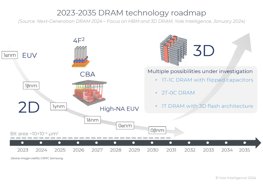
Although currently still finding its way, monolithic 3D DRAM is the foremost long-term scaling solution. Many critical aspects of 3D-DRAM development are as yet unknown, and the way-to-go strategy has not yet been defined. Based on technical papers and patent filings, DRAM companies are exploring many possible pathways to implement monolithic 3D-DRAM, among which are 1T-1C cells with horizontal capacitors, and capacitor-less options, such as gain cells (2T0C) or 1T-DRAM (e.g., based on the floating-body effect). The 2D-to-3D DRAM transition will trigger significant transformations in the DRAM industry that could essentially mimic the history of 3D NAND. Our current market model assumes that 3D DRAM will hit the market in ~2030 and will take about five years to reach ~10 mwpy (38% of the forecasted DRAM wafer production in 2035).

Advanced packaging techniques for DRAM-logic integration and DRAM scaling alternatives to conventional lithography shrinks will be the focus of intense R&D activity by Chinese companies in the coming years. These pathways are currently open – there are no major roadblocks due to commercial restrictions at this stage – and China will follow them to develop high-performance AI chips without making use of restricted leading-edge equipment.* By leveraging More-than-Moore solutions that combine logic and memory, China will remain in the race for technology supremacy in various fields, among which is the critical sector of AI computing.
*Note: 3D DRAM will use “relaxed” lithography nodes (e.g., 20nm) and will not require EUV lithographic systems. We expect that more than 70% of the equipment spend on 3D DRAM manufacturing could be focused on deposition and etching systems.

 www.yolegroup.com
Key Features
- Overview of the semiconductor memory market with focus on DRAM.
- Description of key technology trends and R&D activities by suppliers, such as CBA and 4F2 DRAM, monolithic 3D DRAM, processing-in-memory (PiM) and HBM.
- Market forecast for DRAM in terms of wafer production, bit shipments, bit demand, capex and more.
- Analysis of ongoing and future DRAM technology transitions, such as DDR4-to-DDR5, monolithic 3D DRAM, HBM with hybrid bonding, etc.
- Technology roadmaps by DRAM suppliers and detailed analysis the competitive landscape with focus on China.
- Description of the DRAM ecosystem and analysis of the WFE and material for DRAM manufacturing.
SPRING HAS FINALLY SPRUNG IN THE DRAM BUSINESS! GENERATIVE AI AND HBM WILL FUEL THE MARKET GROWTH.
During the memory market “winter,” demand for DRAM bits remained weak except for some specific applications such as AI servers and automotive electronics. In particular, the rise of generative AI applications from late 2022 (e.g., ChatGPT) boosted demand for high-speed memory technologies – namely DDR5 DRAM and high-bandwidth memory (HBM) – in the data center market.To take advantage of the new generative-AI wave and speed up the market recovery, Samsung, SK hynix, and Micron started diverting more of their wafer capacity to address HBM opportunities, leading to an overall bit production slowdown* and accelerating the shift to undersupply for non-HBM products. The overall HBM wafer production is expected to grow more than 100% YoY in 2024, reaching ~150 kwpm.
Driven by strong demand for AI computing, HBM will largely outgrow the overall DRAM market. After impressive bit-shipment growth in 2023 (+93% YoY), HBM bits are expected to continue growing vigorously in 2024 (+147% YoY) and throughout the next five years (~45% CAGR23-29); by comparison, data center DRAM bits will have a ~25% CAGR23-29. In terms of revenue, the HBM market has the potential to grow from ~$2.7B in 2022 to ~$14B in 2024, corresponding to ~3% and ~19%, respectively, of the overall DRAM revenue.
4F2 CELL DESIGNS, HYBRID BONDING AND MONOLITHIC 3D DRAM WILL ENABLE LONG-TERM DRAM SCALING
4F2 DRAM is currently being developed to reduce chip area by approximately 30% compared to existing 6F2 structures without the need to use smaller lithography nodes. In addition, CMOS-Bonded Array (CBA) DRAM architectures – where the periphery circuit and the memory array are processed on different wafers and then stacked together with wafer-to-wafer hybrid bonding – will be adopted upon introduction of 4F2 cells from ~2027.Hybrid bonding will also be needed for HBM to continue improving memory bandwidth and power efficiency, as well as to minimize HBM stack thickness. We expect that the adoption of hybrid bonding will begin with the HBM4 generation (~2026), which will feature 16 DRAM dies per stack, a 2× increase in interface width up to 2,048 bits.
Although currently still finding its way, monolithic 3D DRAM is the foremost long-term scaling solution. Many critical aspects of 3D-DRAM development are as yet unknown, and the way-to-go strategy has not yet been defined. Based on technical papers and patent filings, DRAM companies are exploring many possible pathways to implement monolithic 3D-DRAM, among which are 1T-1C cells with horizontal capacitors, and capacitor-less options, such as gain cells (2T0C) or 1T-DRAM (e.g., based on the floating-body effect). The 2D-to-3D DRAM transition will trigger significant transformations in the DRAM industry that could essentially mimic the history of 3D NAND. Our current market model assumes that 3D DRAM will hit the market in ~2030 and will take about five years to reach ~10 mwpy (38% of the forecasted DRAM wafer production in 2035).
THE FIGHT FOR LEADERSHIP IN HBM IS SET TO ESCALATE. IN THE LONG TERM, THE SHIFT TO 3D WILL OPEN NEW OPPORTUNITIES FOR CHINA.
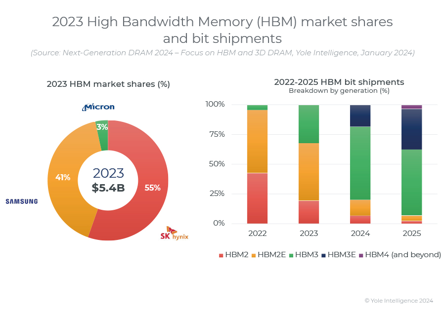
Since 2013, SK hynix has been a pioneer in the development and commercialization of HBM and currently leads the HBM market with ~55% revenue share, followed by Samsung with ~41%. Micron was noticeably absent from HBM until 2020. As a late entrant to the HBM business, this American company needs to reduce the time to market, and for this purpose, they will skip the HBM3 generation and introduce directly HBM3E products (aka HBM3 Gen 2).Advanced packaging techniques for DRAM-logic integration and DRAM scaling alternatives to conventional lithography shrinks will be the focus of intense R&D activity by Chinese companies in the coming years. These pathways are currently open – there are no major roadblocks due to commercial restrictions at this stage – and China will follow them to develop high-performance AI chips without making use of restricted leading-edge equipment.* By leveraging More-than-Moore solutions that combine logic and memory, China will remain in the race for technology supremacy in various fields, among which is the critical sector of AI computing.
*Note: 3D DRAM will use “relaxed” lithography nodes (e.g., 20nm) and will not require EUV lithographic systems. We expect that more than 70% of the equipment spend on 3D DRAM manufacturing could be focused on deposition and etching systems.
Yole Group - Follow the latest trend news in the Semiconductor Industry
Yole Group - Access daily business, market & technology updates in the semiconductor industry, our Analysts' Analysis and Presentations and more

