You are currently viewing SemiWiki as a guest which gives you limited access to the site. To view blog comments and experience other SemiWiki features you must be a registered member. Registration is fast, simple, and absolutely free so please, join our community today!
It is too soon to tell but I'm sure this guy got some big clicks.
"OK, maybe Apple didn't want to push the boat out on transistor count this time and wanted to keep costs in check."
Apple wanted to keep SOC costs in check? Hahahahaha Never happened!!!!!!
It will be interesting to see the difference between the Apple N5 SOC, the Apple N4 SoC, and the Apple N3 SoC. Looking forward to the TechInsights tear down.
The A17 and iPhone will sell like hot cakes. Clearly with demand for 3nm it must be offering something to all the fabless.
The line is long for future customers as will the adopters leading to another win and further leadership and competitive MOAT for them. Only the armchair technologist looking for clicks have no clue
Products on a new node normally seem to underwhelm a little bit. See Broadwell on Intel 14nm, icelake on Intel 10nm, or even the Apple SoC that led TSMC N5. When GPUs were leading nodes a long time ago we saw some of the same at the various foundries.
No need to worry unless we still see small improvements over N5 in 18 months.
People are looking at this the wrong way, If you are looking at CPU performance by traditional measures, yes not much improvement. But this isn't Apple's focus. There has been a huge increase in performance of neural engine and GPU, less increase in CPU. This is not captured by these benchmarks.
Actually N3P (a tweaked 2% linear shrink of N3E) is looking more likely to be "the big one" -- I heard from our digital team that TSMC has upset a lot of people by accelerating the N3P schedule and short-cutting N3E, as a consequence everyone is moving to N3P while complaining that the libraries aren't available...
N3X is targeted at CPUs where short-term burst maximum speed at raised voltage is the priority, it's not suitable for applications where power efficiency and long lifetime at full clock rate matter.
People are looking at this the wrong way, If you are looking at CPU performance by traditional measures, yes not much improvement. But this isn't Apple's focus. There has been a huge increase in performance of neural engine and GPU, less increase in CPU. This is not captured by these benchmarks.
That what I was kind of saying. If you a limited number of chip architecture / design staff, you probably would focus them on NPU, GPU, video/image processing, and misc accelerators rather than improving your CPU cores. I presume having bragging rights for significantly faster cpu than the previous year is low on Apple’s priorities.
Being on the latest node lets you cram more for less space to take advantage of less power.
Apple's iPhone 15 Pro will be the first smartphone to use TSMC's N3 process, offering new features like powerful graphics. Find out if AAPL stock is a buy.
Ya. CPU cores are less important on mobile phones than GPU, NPU and built in codec support.
That what I was kind of saying. If you a limited number of chip architecture / design staff, you probably would focus them on NPU, GPU, video/image processing, and misc accelerators rather than improving your CPU cores. I presume having bragging rights for significantly faster cpu than the previous year is low on Apple’s priorities.
Being on the latest node lets you cram more for less space to take advantage of less power.
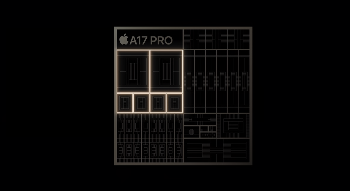
I think the thing that had folk's panties in a bunch was the modest transistor count increase relative to the advertised density. Although I think most of these folks miss that due to the extended stay at N4 die sizes bloated up. Makes sense that on the new node Apple would want to go back to "the good old days" of sub 100mm^2 dies.
Actually N3P (a tweaked 2% linear shrink of N3E) is looking more likely to be "the big one" -- I heard from our digital team that TSMC has upset a lot of people by accelerating the N3P schedule and short-cutting N3E, as a consequence everyone is moving to N3P while complaining that the libraries aren't available...
N3X is targeted at CPUs where short-term burst maximum speed at raised voltage is the priority, it's not suitable for applications where power efficiency and long lifetime at full clock rate matter.
I think the thing that had folk's panties in a bunch was the modest transistor count increase relative to the advertised density. Although I think most of these folks miss that due to the extended stay at N4 die sizes bloated up. Makes sense that on the new node Apple would want to go back to "the good old days" of sub 100mm^2 dies.
Yes. Very true. Square mm size is probably down to 65-75. The N3B node was a little less than double the what the previous N4 node cost, if I remember correctly. This leaves Apple a chance to grow the total area size of their SoCs by the time they used the final N3 node (N3P, N3S, or whatever it ends up being).
I was thinking along the same lines as the seeking alpha article linked above. My mental math about SoC area is probably off though.
I thought that TSMC previously indicated that N3E would contain lower density when compared to the N3 node. As based on my prior understanding N3E was exclusively designed for facilitating the availability of a more commercially viable node.
I thought that TSMC previously indicated that N3E would contain lower density when compared to the N3 node. As based on my prior understanding N3E was exclusively designed for facilitating the availability of a more commercially viable node.
And that would be why. Obviously N3 is a more mature process than N3E at the moment. But I would have to assume that either at an equivalent maturity level N3E will yield better or at the very least will have a lower DD floor than N3. Costs per wafer and cycle times would also be lower, as will tapeout costs due to fewer euv mask sets. Performance per watt is also better on N3E family. As you say, density is lower and that is the question mark. TSMC says finflex exists for N3, but they don’t specify if the 1.7x number is the 2-1 library or the 2-2 library. If it was using the former then N3E is truly a no brainer improvement with an insignificant density hit. If it is the later then it is much harder to say if N3E would be a cost per fet decrease compared to N3. However it seems pretty reasonable that customers (especially those who make big dies or only want a hyper mature node on deprecated tools) would be willing to swallow a worse cost per fet for the listed benefits (as they kind of do that anyways by staying off the bleeding edge nodes).
Planar ran out of steam, forcing the transition to FinFET. FinFET is now delivering diminishing returns, forcing the transition to GAA. So there should be no surprise that N3 is not a great leap forward...
Planar ran out of steam, forcing the transition to FinFET. FinFET is now delivering diminishing returns, forcing the transition to GAA. So there should be no surprise that N3 is not a great leap forward...
We stopped doing giant leaps years ago when we had 2-3-4 years between new nodes. 5-10% performance increase every year is not bad, right? GAA (HNS) will be the same. Incremental increases every year or two then we go to CFETs.
But, do we really need big performance gains for SoCs in phones? Not for what I use them for. Connectivity is the big deal for me. I need more bars when I'm sailing!
Actually N3P (a tweaked 2% linear shrink of N3E) is looking more likely to be "the big one" -- I heard from our digital team that TSMC has upset a lot of people by accelerating the N3P schedule and short-cutting N3E, as a consequence everyone is moving to N3P while complaining that the libraries aren't available...
N3X is targeted at CPUs where short-term burst maximum speed at raised voltage is the priority, it's not suitable for applications where power efficiency and long lifetime at full clock rate matter.
We stopped doing giant leaps years ago when we had 2-3-4 years between new nodes. 5-10% performance increase every year is not bad, right? GAA (HNS) will be the same. Incremental increases every year or two then we go to CFETs.
But, do we really need big performance gains for SoCs in phones? Not for what I use them for. Connectivity is the big deal for me. I need more bars when I'm sailing!

 www.pcgamer.com