At IEDM23 we got to get a glimpse at the early enabling work for the big three’s CFET technology. One thing I found very interesting was the seemingly different research priorities.
Samsung in someways had simultaneously the most and least impressive showing. They showed off a CFET device with tighter cpp than even N3B. But unfortunately they lacked the extra sauce to go with it (at least based on the synopsis listed below as I haven’t yet gotten the chance to read Samsung’s full paper). As far as I know this is also the first time Samsung has showed off real CFET devices.
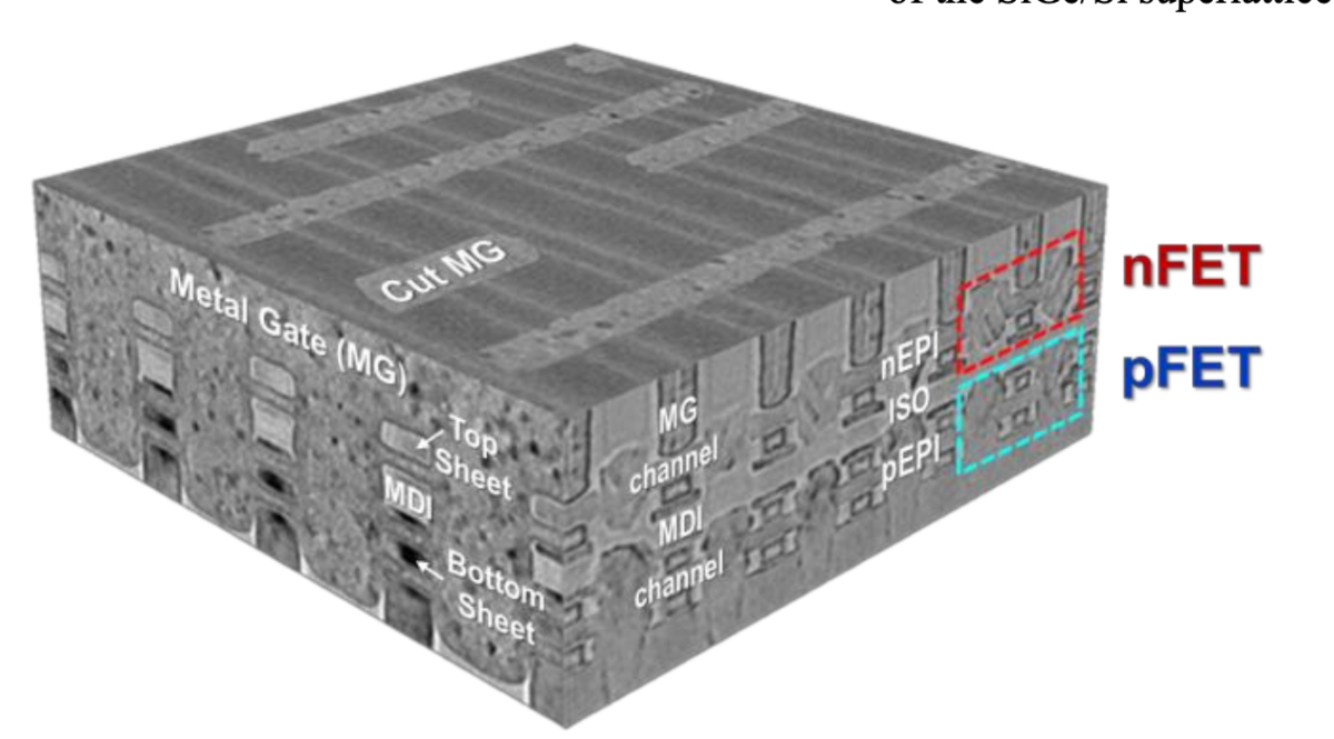
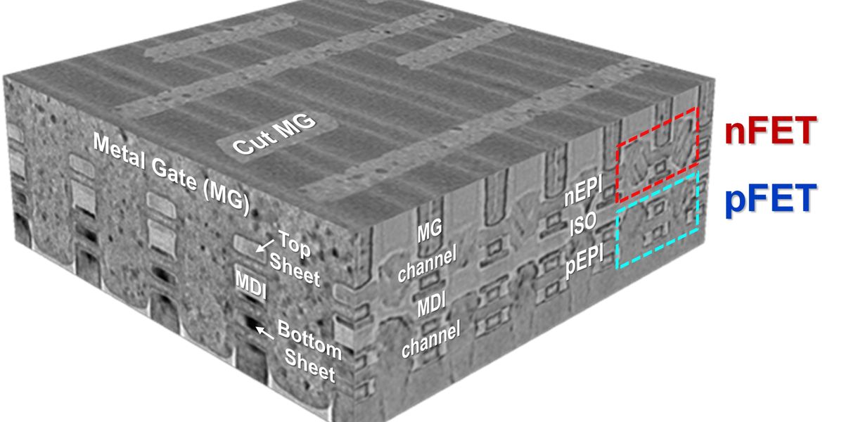
TSMC for their part wasn’t very far behind on poly pitch with 48pp cells that are likely similar to what we will see on N3E. They also had a nifty dielectric isolation that feels reminiscent of forksheet FET as well as N3B’s gate endcap. I am not sure how you would go about doing devices with merged gates without using another litho and epi pass so that lower Ge content SiGe gets deped for the cells that want a common gate. Either way it gets two thumbs up from me as I am actually quite fond of the concept behind forksheet FETs.
Not to be left out intel has also updated us on their developments. In this work they were keeping the poly pitch very loose at 60nm. However they extended their 2 sheets lead to a 3 sheet lead vs everyone else’s CFETs. Unsurprisingly intel has also made sure to market their lead in BSPD and even showcased fully integrated circuits (specifically inverters). Besides the obvious gate shrinkage, one area of improvement seemed to be doing the enabling work for more complex circuitry.
All told very interesting that Samsung is prioritizing getting the device down to production like pitches. TSMC has a similar focus with a greater focus on yield as their dielectric wall should greatly help with GtG shorts. Intel for its part seems to be focusing on creating a transistor architecture that is ready for the prime time and then shrinking from there.
 spectrum.ieee.org
Samsung in someways had simultaneously the most and least impressive showing. They showed off a CFET device with tighter cpp than even N3B. But unfortunately they lacked the extra sauce to go with it (at least based on the synopsis listed below as I haven’t yet gotten the chance to read Samsung’s full paper). As far as I know this is also the first time Samsung has showed off real CFET devices.
TSMC for their part wasn’t very far behind on poly pitch with 48pp cells that are likely similar to what we will see on N3E. They also had a nifty dielectric isolation that feels reminiscent of forksheet FET as well as N3B’s gate endcap. I am not sure how you would go about doing devices with merged gates without using another litho and epi pass so that lower Ge content SiGe gets deped for the cells that want a common gate. Either way it gets two thumbs up from me as I am actually quite fond of the concept behind forksheet FETs.
Not to be left out intel has also updated us on their developments. In this work they were keeping the poly pitch very loose at 60nm. However they extended their 2 sheets lead to a 3 sheet lead vs everyone else’s CFETs. Unsurprisingly intel has also made sure to market their lead in BSPD and even showcased fully integrated circuits (specifically inverters). Besides the obvious gate shrinkage, one area of improvement seemed to be doing the enabling work for more complex circuitry.
All told very interesting that Samsung is prioritizing getting the device down to production like pitches. TSMC has a similar focus with a greater focus on yield as their dielectric wall should greatly help with GtG shorts. Intel for its part seems to be focusing on creating a transistor architecture that is ready for the prime time and then shrinking from there.
Intel, Samsung, and TSMC Demo 3D-Stacked Transistors
The Big Three can now all make CFETs—next stop on the Moore’s Law roadmap
spectrum.ieee.org