When I first moved to Oregon in 1978 the largest industry was forestry, but then the endangered Spotted Owl was found and that put an end to many forestry companies and decimated the economy of many rural cities. Strangely enough it turns out that the Spotted Owl was found in great numbers across multiple states, so it never should’ve been placed on the endangered species list in the first place. Fast forward to 2015 and the number one Oregon industry is semiconductors, with Intel at the top revenue position. Many Californians have made the move to Oregon because housing is affordable in the Silicon Forest, the air is clean, and our Pinot Noir wines are world-class.
SEMIis a global industry association and they just hosted an event in Wilsonville (aka Mentor Graphics) with over 150 techies in attendance, the theme was Moore’s Law and I attended after a short 7 mile drive from Tualatin.
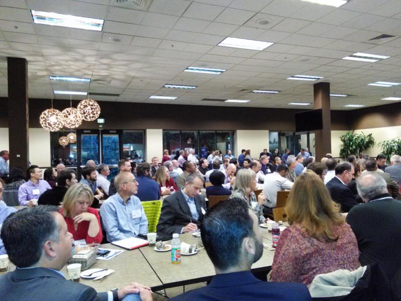
Mentor Graphics
Wally Rhines waxed energetically about extending semiconductor cost reduction for another 20 years, although even Gordon Moore is quoted as saying that, “No exponential is forever”. Here’s the log-log chart defining the learning curve where the X-Axis is cumulative units produced and the Y-axis is cost per unit:
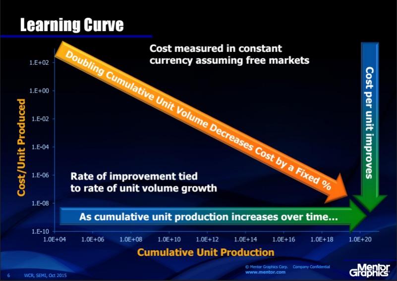
Rhines showed historical data that followed this exact curve for:
- Revenue per transistor versus cumulative transistors shipped
- Personal computer volume
- Revenue per MIPS
- Semi equipment supplier
- Photolithography equipment
- Assembly equipment
- ATE
- EDA tools
In general Wally has seen that EDA revenue is about 2% of total Semiconductor revenues over the past 20 years now.
The costs per wafer show about a 20% increase per new node, but at the 20nm node the costs were more expensive than 28nm per transistor. At 14nm the cost per transistor still too high because we’ve missed the commercialization of EUV sources. In spite of all that, he expects that we’ll have continued progress per Moore’s Law for another decade.
ASML
Chris Spence started out by humorously apologizing for EUV being late to market, then presented an info-packed slide on 30 years of Litho progress.
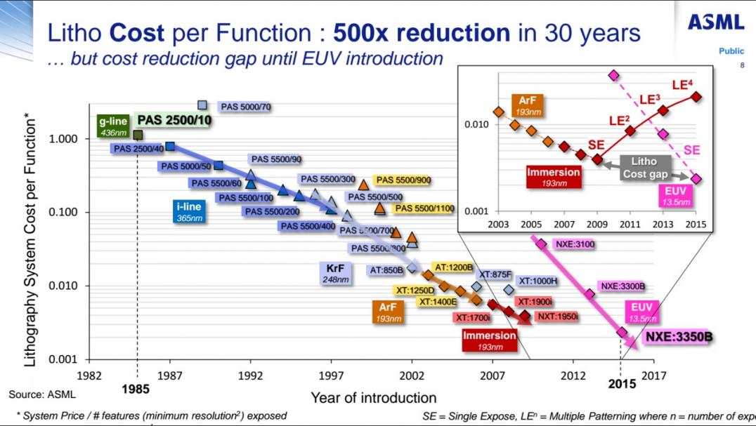
EUV is still beset by slow throughput as measured in Wafers Per Hour (WPH) and high costs. ASML’s 3rd generation EUV tool, the NXE 3350B, can product up to 125 WPH, it’s progress but it isn’t easy
Defects can be related to IC layout patterns, not defect particles, so OPC can predict those patterns with a tool like Tachyon. Yes, multi-patterning allows us to reach lower than 10nm, however it will be pricey.
INTEL
Our speaker from the supply chain side was David Bloss, and he was quick to emphasize that, “Moore’s law is thriving at Intel”. The most controversial thing that David shared was that Intel has found a way to make cheaper transistors at 22nm and smaller nodes, contrary to what the rest of the industry seems to be saying. Their 7nm node is about a decade out, so that means 2025.
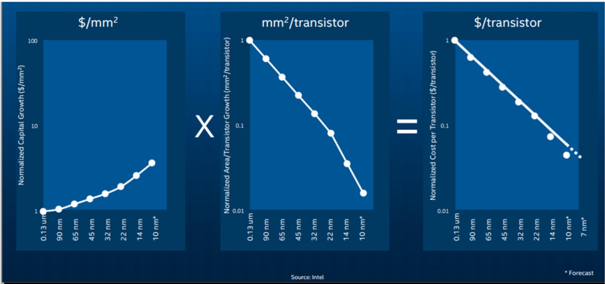
This slide is from Bill Holt’s investor meeting presentation of November 2014, one year ago. Intel was pleased that their suppliers are helping make Moore’s Law continue on. As for 450mm wafers we can expect that Intel will wait for the industry to drive demand.
IBM
From the R&D side we had Dr. Vamsi Paruchuri talking about the materials and process technology for advanced CMOS nodes. Although I don’t have permission to show you any of the slides that Vamsi presented, I can show you the IBM 7nm test chip that came out of fab in July, designed with silicon germanium for FinFET transistors, using EUV to get the small geometries.
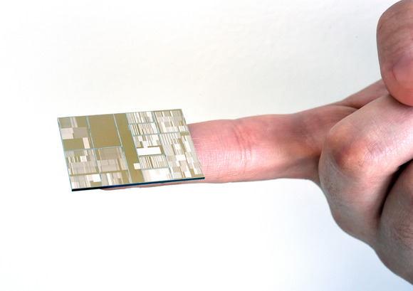
Credit: Darryl Bautista/IBM
I found it interest that at the 7nm node they needed to use SiGe channels on FinFET for lower power and faster switching. Gate lengths are 15nm in 7nm technology, transistor width is 8nm minimum, and the height is 20nm.
Other interesting research technologies include Si Nanowire, Carbon Electronics (Carbon Nanotubes – optics and semi together), III IV FinFet, Stacked Nanowires, Stacked Nanosheet, and Gate All Around FinFET (GAAFET).
ASE
Representing the package and assembly business we heard from John Hunt. The hot acronym to remember is for Wafer Level Chip Scale Package, WLCSP.
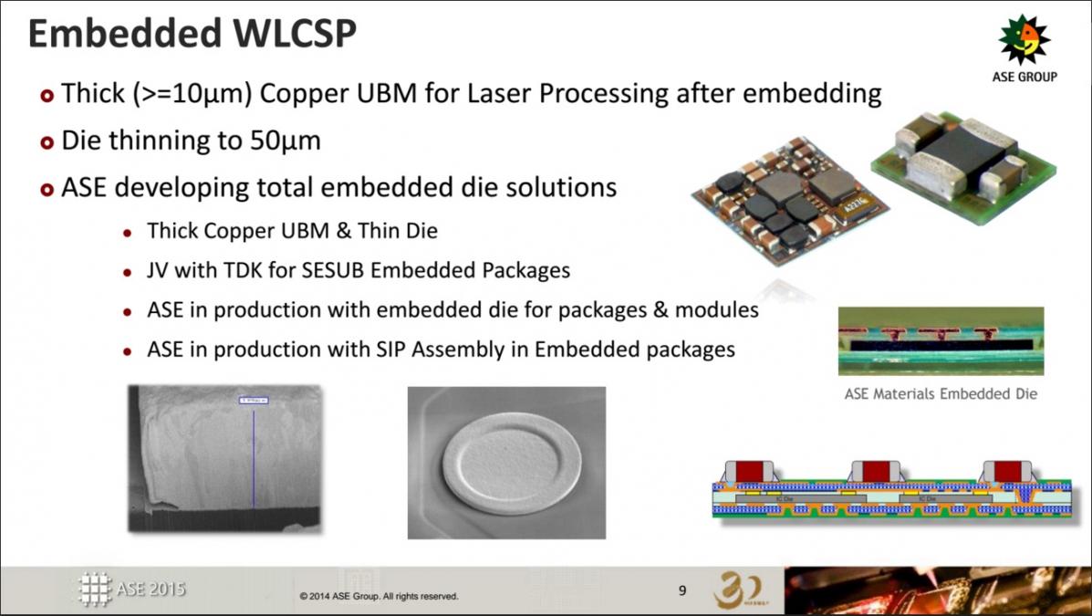
Popular consumer devices like the Apple Watch and iPhone will be using technology like WLCSP to enable extremely thin products. TSMC will build the Apple A10 with fanout packaging technology. For IoT devices you can expect to see Fan Out SiP (System in Package).
Yole Development
Dave Towne showed us how more than Moore is being enabled by advanced packaging. Yole Development has standard reports for sale, custom research reports, and they know the market trends. On Fan Out Wafer Level Packaging (FOWLP) they are predicting this market segment to grow from $174M this year to $790M next year when the A10 is announced from Apple and using TSMC for both the chip and packaging technology. TSMC calls this Integrated Fan Out (InFO).
Take a quick look at how 2D versus 3D packaging features compare:
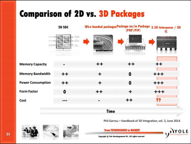
Source: Yole Development
Mobile phone companies like Apple and Samsung are routinely using Wafer Level Packaging to achieve the thinnest integrations. CMOS Image sensors are a big user of 3D packaging, and that trend continues on strongly.
Summary
It was a pleasant surprise to be exposed to such diverse presentations from SEMI members in one setting, because I normally have my EDA blinders on and get too focused on software-only solutions to semiconductor design challenges. It was clear that all of these companies must collaborate closely in order to exploit everything that silicon has to offer us. For now, Moore’s Law continues and the only question is, “At what cost per transistor?”
Don’t forget to follow SemiWiki on LinkedIn HERE…Thank you for your support!
Share this post via:


Comments
0 Replies to “Moore’s Law and Silicon Forest”
You must register or log in to view/post comments.