In an overwhelmingly digital world, there is a constant cry about the analog design process being slow, not automated, going at its own pace in the same old fashion, and so on. And, the analog world is not happy with the way it’s getting dragged into imperfect automation so it can be more like the digital world. True, the analog world loves perfection; do the process according to its needs and it’s happy. So, do we have an environment where we can accommodate the persistent demand from the analog world for preserving its unique identity and still deliver the required productivity improvement?


Since SpringSoft, a provider of custom layout tools, was acquired by Synopsysabout three years ago, I’ve wanted to find out what the digital giant has been doing to automate analog design. I found a great opportunity to talk to my long-time former colleagues Fred Sendig, Fellow at Synopsys and Dave Reed, Product Marketing Director at Synopsys. Fred is a well known technologist in the analog/mixed signal space that I worked closely with in my Cadence days. This meeting was an eye-opener to another level of innovation in the making from Synopsys, only this time, in the analog/custom design world. Instead of promising to fully automate analog design – something analog designers have long resisted — Synopsys’ vision is based on the concept of design assistance.
In the analog world, designer productivity counts more than anything else; automation can’t help if a designer has to redo the things to make the design perfect. Today, the custom design challenge has significantly increased with the introduction of FinFETs at lower nodes. Multi-patterning is required in the fabrication processes. The number of design rules and their complexities has increased significantly. The FinFET-based devices exhibit higher parasitic capacitances, and a higher resistance in local interconnect at lower-level metal layers. The device is more vulnerable to electro-migration due to extremely thin interconnect. Also, in FinFET designs, one device in the schematic can map to multiple FinFETs connected together in a complex series and/or parallel pattern to achieve desired design strength. So, the layout of even a simple circuit such as a differential pair may require the placement of hundreds of individual FinFET devices in complex matching patterns. It’s evident that automation is needed to counter such complexity and increased work, but how should it be done without violating designers’ intent and while keeping them happy?
Synopsys envisions preserving designers’ complete control over the layout and providing assisted automation to help increase productivity by 3X or more. The custom design environment envisioned by Synopsys will have several productivity boosters including:
- Storing and reusing placement patterns and prior building blocks with further customization options
- Using up-front knowledge of physical and electrical effects
- Less effort required for creation and optimization, thus allowing designers to work at a higher level without losing their focus on the differentiating aspects of their design at the circuit and layout stages. In this way, the designs will be made perfect as early as possible in the design cycle to reduce the number of engineering change orders (ECOs).
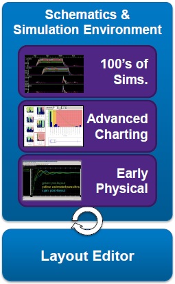
 The Synopsys vision for this custom design platform has circuit design and layout implementation flows working in a closed loop. The circuit design flow would let designers start from design entry and quickly converge on the final layout with a minimum number of ECOs. There would be fast extraction and simulation engines for quick analysis of electro-migration, IR drop, parasitics, etc. for the layout at different corners and its optimization for the best power, performance and area. There would be advanced analysis features to manage results from hundreds of corners.

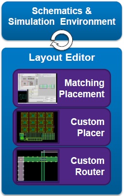
The matching placement would keep the designer’s intent intact in the layout. The designer would then have the flexibility to modify it further according to her/his needs. The custom placer and router would perform automatic placement and routing of the devices. The electrical verification could be done during the layout. The physical simulation could be done at any stage before completion of the layout. This flexibility would deliver faster turn-around after any ECO in the layout.
Synopsysexpects to see ~3x productivity improvement in custom layout design with this approach compared to earlier solutions. Their IP design team has already been using this assisted custom automation flow at advanced process nodes. Synopsys’ MSIP team taped out several FinFET-based designs including USBs, DDRs, PCIe buses, HDMI, DPHY, and others at TSMC16FFP LL/GL and Samsung 14LPE and LPP.
Synopsys’ new custom design methodology is driven by the increasing challenges in FinFET technology at lower nodes and by customer demand for improved designer productivity. The solution is already in progress and there are several beta customers using it. It will be interesting to see this methodology rolled out. Assisted automation will be an important and effective upgrade for analog designs in the custom design space.
Pawan Kumar Fangaria
Founder & President at www.fangarias.com


Comments
0 Replies to “Synopsys Vision on Custom Automation with FinFET”
You must register or log in to view/post comments.