
")
Complexity and density conspire to make power delivery very difficult for advanced SoCs. Signal integrity, power integrity, reliability and heat can seem to present unsolvable problems when it comes to efficient power management. There is just not enough room to get it all done with the routing layers available on the top side of the chip. A strategy is emerging to deal with the problem that seems to take a page out of the multi-die playbook. Rather than deal with the existing, single surface constraints, why not move power delivery to the backside of the chip, and get additional PPA benefit out of it? The entire fab and process equipment ecosystem is buzzing about this approach. But what about the design methodology? There is help on the way. A very informative white paper is now available from the leading EDA supplier. Read on to get the details about how Synopsys enhances PPA with backside routing.
Why Use BackSide Routing?
In a typical SOC, dedicated power layers tend to be thicker, with wider traces than the signal layers to reduce the amount of loss due to IR drop. The power delivery network, or PDN, is what brings power to all parts of the chip. PDN design required extensive analysis of electromigration, noise, and cross-coupling effects as well as IR drop to ensure power integrity. Solving this problem by adding metal layers will increases the cost and complexity of the fabrication process, if it’s even possible given process constraints.
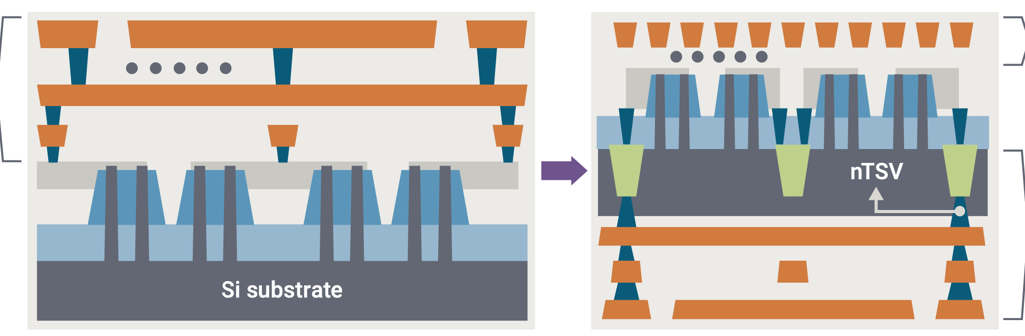
There is more to the story which is explained well in the white paper (a link is coming). Now that manufacturing technology supports it, backside routing for the PDN is a great way to remove the obstacles, opening a new approach to implementation and the opportunity to enhance PPA. The graphic at the top of this post provides a comparison of frontside and backside PDNs. Thanks to IMEC for this depiction.
But, as they say, there’s no free lunch. For backside routing, the design process has to deal with many new problems, such as:
- Signal integrity
- Frontside PDN acted as a natural shield for signal integrity
- Important to have close correlation between pre-route and post-route
- Thermal impact
- Thermal aware implementation to reduce impact of backside metal
- Post-silicon observability
- Methodologies to support robust observability
- Multi-die and backside metal
- Lots of synergy between the two
- Leverage EDA technology pieces from each other
The white paper also explains what Synopsys is doing for backside routing. Here is a summary.
What Synopsys is Doing
Synopsys has embraced the use of backside routing for the PDN. The approach fits well with its design technology co-optimization (DTCO) methodology. The company has added support for backside PDNs in all relevant EDA products. The result is fast and efficient technology exploration, design PPA assessment, and design closure to accelerate the overall development process. As with many of its programs, the approach allows chip designers to adopt new silicon technology with predictable results.
A large number of additions are part of Synopsys Fusion Compiler, the industry-leading RTL-to-GDSII implementation system. The figure below summarizes the enhancement at a high level. The white paper goes into more detail about these enhancements and the measurable impact on chip design results.

The white paper also discusses potential future additions to expand the use of backside routing even further.
To Learn More
Backside routing is here. The foundry ecosystem is delivering this capability and design teams need an enhanced flow to take advantage of the benefits, both today and tomorrow. Synopsys is at the leading edge of this trend and the new white paper provides important details. You can get a copy of the new Synopsys white paper here. And that’s how Synopsys enhances PPA with backside routing.
Share this post via:


Comments
There are no comments yet.
You must register or log in to view/post comments.