You are currently viewing SemiWiki as a guest which gives you limited access to the site. To view blog comments and experience other SemiWiki features you must be a registered member. Registration is fast, simple, and absolutely free so please,
join our community today!
Power densities on chips increased from 50-100 W/cm2 in 2010 to 200 W/cm2 in 2020, creating a significant challenge in removing and spreading heat to ensure reliable chip operation. The DAC 2025 panel discussion on new cooling strategies for future computing featured experts from NVIDIA Research, Cadence, ESL/EPFL, the University… Read More
Bruce Caryl is a Product Specialist with Siemens EDA
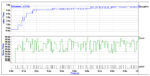
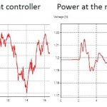
The most common way to evaluate a power distribution network is to look at its impedance over the effective frequency range. A lower impedance will produce less noise when transient current is demanded by the IC output buffers. However, this transient current needs to be provided… Read More
High-speed PCB designs are complex, often requiring a team with design engineers, PCB designers and SI/PI engineers working together to produce a reliable product, delivered on time and within budget. Cadence has been offering PCB tools for many years, and they recently wrote a 10-page white paper on this topic, so I’ll share … Read More
For advanced semiconductor designs, achieving both design rule check clean layouts and optimal electrical performance is crucial for minimizing design iterations, reducing time-to-market and ensuring product reliability. Balancing electrical performance and layout integrity is a difficult task. Achieving an optimal… Read More
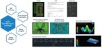
Signal Integrity (SI) and Power Integrity (PI) issues are critical to analyze, ensuring the proper operation of PCB systems and IC packages, yet the computational demands from EDA tools can cause engineers to only analyze what they deem are critical signals, instead of the entire system. Cadence has managed to overcome this SI/PI… Read More
Complexity and density conspire to make power delivery very difficult for advanced SoCs. Signal integrity, power integrity, reliability and heat can seem to present unsolvable problems when it comes to efficient power management. There is just not enough room to get it all done with the routing layers available on the top side… Read More
Counting squares is a useful tool for calculating simple resistance in wires, but falls short in reality when wires deviate from ideal. Frequently the use of RC extraction tools for determining resistance in signal lines in digital designs can be effective and straightforward. However, there are classes of nets in designs that… Read More
2015 will be remembered as the year when chip-package-system (CPS) physical co-design and electrical/thermal analysis methodologies took center stage.… Read More
DesignCon is a unique conference — its tagline is “Where the Chip meets the Board”. Held each January in Santa Clara, the conference showcases a wealth of new technologies for advanced packaging, printed circuit board fabrication, connectors, cables, and related analysis equipment (e.g, BERT, VNA, scopes). Of specific… Read More
The way we are seeing technology progression these days is unprecedented. It’s just about six months ago, I had written about the intense collaboration between ANSYSand TSMCon the 16nm FinFET based design flow and TSMC certifying ANSYS tools for TSMC 16nm FF+ technology and also conferring ANSYS with “Partner of the Year” award.… Read More