 At CDNLive Silicon Valley 2018, I talked with Yuval Shay, Director of Product Management of Cadence Custom IC & PCB Group to scope out some more details on the recent Virtuoso product refresh announced earlier in the morning by Cadence Sr. VP & GM of the same group, Tom Beckley.
Tom shared his view on enabling the fourth industrial revolution (4IR). He illustrated the challenges faced by both the system and the semiconductor companies such as the growing need for complex integration across chip, package and board; the use of advanced technologies; designing systems that constantly connected to the cloud through the emerging 5G standard; and the changes in the automotive industry with autonomous cars.
Elaborating further, Tom talked about System Design Enablement (SDE) and the effort his organization is putting into SDE as well as how Virtuoso is enhanced to help address the challenges designing complex systems.
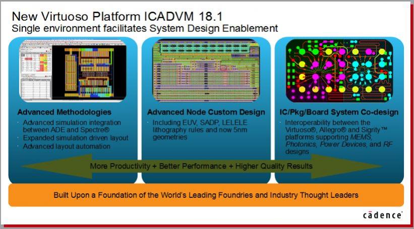
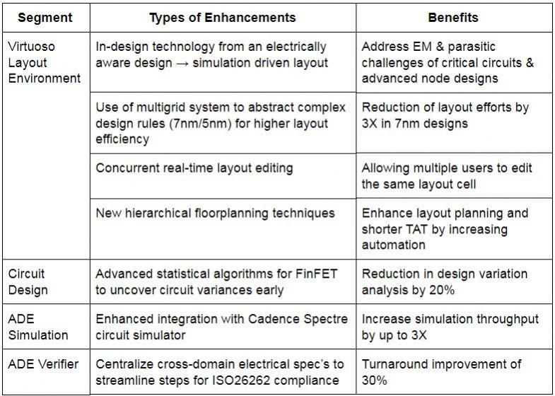
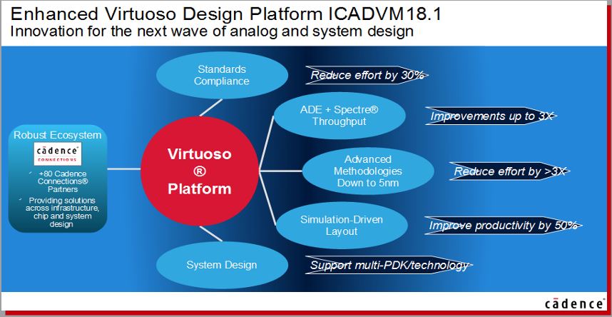
Yuval provided some Virtuoso press-release materials, which are also used as reference for my interview. In this release, Cadence revamped the Virtuoso design platform, dubbed ICADVM 18.1 to include the following updates, delivering productivity improvement across multiple segments.


Commenting on the announcement for Virtuoso upgrades that include feature to 5nm process support, Yuval first articulated the increased complexity of system’s integration and the effort to driving down system’s costs. For example, ADAS application with LIDAR technology, combining laser diode, MEMS, photonics, analog sensors and advanced node SOC’s –all integrated into a single system to provide a sub-$100 LIDAR system. Not only leading providers need a state of the art IC tools and solution across multiple technologies, customers also need system solutions.

Tell me about Virtuoso System Design Platform, and what’s new in ICADV18.1 ?
We first introduced Virtuoso System Design Platform (VSDP) in May 2017. It was an immediate hit; the rate of adoption is amazing. Only few months since the announcement and already customers using it in production. It showed us how strong the need is.
What VSDP really does, is allowing a “golden” schematic to capture the system design (SIP) using Virtuoso Schematic Editor and to drive downstream applications. Using Virtuoso’s schematic, the environment can drive Cadence SIP tool for layout implementation, automating the layout-versus-schematic (LVS) verification flow. At the same time, analysis done on the SIP layout, using Sigrity 3D-EM extraction and generating parasitics models, can be back-annotated into Virtuoso. Virtuoso will automatically manage the simulation environment, eliminating the highly manual and error-prone process of integrating system-level layout parasitic models back into the IC designer’s flow. All of this done by maintaining a single “Golden” schematic for both LVS and verification.
New in Virtuoso ICADVM18.1, is the ability to edit the SIP layout using Virtuoso Layout Suite and to be able to edit each die in the SIP layout and managing multiple process Design Kits (PDK’s), simultaneously.
Could you comment about concurrent layout access which was mentioned in the keynote?
Custom IC design depends on hierarchical design methodology, where each layout hierarchy (cellview) can be edited by a single user at a time. For example, if during sign-off review, there are thousands of DRC violations needed to be fixed at the top level, the ability to distribute the job across multiple users is limited. We developed a new technology which allows for multiple users to edit the same cellview/hierarchy and allow for selective integration of edits back into the master cellview. There is the ability for the cellview owner to accept or reject edits from other users and to add notes, in case edits get rejected. This new technology allows for a non-destructive editing of the layout artwork –data being touched just like editing a picture on your smartphone.
Could you share recent example of ML application in custom design space?
Design integrity and robustness need to be guaranteed for Custom Analog IP’s while designed within a timely manner. Virtuoso’s Electrically Aware Design (EAD) environment enables users to perform parasitics extraction and EM analysis on partial layout. We use Machine Learning (ML) to generate unique technology database with highly trained model for fast extraction of parasitic with high accuracy. Incremental RC extraction can be done within seconds as design being developed. For example, we have a customer using this top-level design with thousands of nets, to check coupling between noisy and sensitive nets to prevent crosstalk. This can be done in-design within seconds. In this new release of Virtuoso, we enhanced our layout environment to be driven by simulation data, introducing for the first time “Simulation Driven Layout” to mitigate EM problems, in-design.
What are the top three challenges in custom design space?
First, in the analog design space, there is a need of increased automation in order to shorten turn-around time. For example, people aspires to do top-down design, floorplanning and explore ways to reduce die-size. In reality, for a given project, there is no time to explore multiple floorplans and run multiple routing jobs to see if a new plan will converge. So designer usually goes with prior design knowledge and floorplan, or make a best educated guess. We developed new capability in Virtuoso to efficiently plan the design hierarchies, floorplan the design and analyze it for congestion and convergence –enabling multiple floorplanning exercises to occur in a short amount of time. This allows designers to find opportunities to do die size reduction.
Second, custom design gets extremely challenging in the advanced node process. Layout effort keeps increasing to a point where there is not adequate PD (Physical Designer) to complete the jobs. We advocate for a smarter methodology to better manage the sheer number of design rules, EM, layer’s density requirements and design variation. Virtuoso has the environment to address all of these. The 3X speed-up in keynote is conservative, in reality it could be even higher.

Third, design is not an isolated (effort) anymore –designers need to care about packaging and packaging effects on their design as well as to have the ability to manage multiple IC’s and complexity of advanced packages including its associated critical effects (for example, parasitic/magnetic on PCB affect IC design). How to capture those effects early, taking SiP design into analysis. We enhanced our Virtuoso System Design Platform to help with those challenges and collaborating with EDA connection partners to help customer with the solution.
Can you highlight a recent customer engagement experience?
At this CDNLive we had Bosch presenting the result of our collaboration on Simulation-Driven Layout. As you can imagine, Bosch care greatly about design reliability and wanted a solution to mitigate electro-migration problems, while not dragging down overall productivity. We worked together on this and came-out with a solution we are proud of. The new environment allows users to examine and plan their layout based on both current flow and current density. In addition, when using Virtuoso Wire Editor, wires will be sized automatically to address current density requirements.
At the end of the interview, I was inquiring about further anticipation of expanding cloud availability similar to the OrCAD Entrepreneur case. He tactfully mentioned Cadence have currently hosted design solution through (design) services and cloud readiness is being considered across Cadence.
Share this post via:


Comments
There are no comments yet.
You must register or log in to view/post comments.