This article will describe the motivations for pursuing a new flow in the SoC design methodology. This flow involves the extraction, evaluation, and analysis of a full electromagnetic coupling model for a complex SoC and its package environment. The results of this analysis highlight the impact of electromagnetic coupling on the performance and functionality of modern-day complex SOC designs.
Background
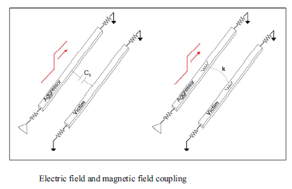
With the introduction of nanometer process scaling, the vertical-to-horizontal aspect ratio of interconnects increased above unity. As a result, the much larger contributions of capacitive crosstalk from a neighboring aggressor to a victim net necessitated new and improved SoC design flows. Noise analysis tools and corresponding IP characterization methods were developed to ensure that the (cumulative) energy injected into a (quiescent) victim net from its aggressors did not subsequently result in a circuit network failure. Algorithms for interconnect delay calculation used in static timing analysis flows were extended to reflect the noise impact on delay, due to the potential waveform modifications at the fanouts of a transitioning signal from concurrent transitions on aggressors.
EDA tools for physical implementation also incorporated new features. Specifically, detailed routing algorithms were extended to include restrictions on the parallel run length of adjacent interconnects. More sophisticated noise calculation/avoidance methods were incorporated to assist with wiring track selection.
Designers also quickly adopted techniques to further mitigate the risk of subsequent capacitive crosstalk noise failures. Specific non-default rules (NDR) for critical nets were coded, to guide implementation tools to use greater-than-minimum spacing between metal segments on a layer and/or to direct segments to a track adjacent to a non-switching (power/ground) net to effectively shield the segment from coupling transitions.
The limited extent of the capacitive electric field lines between metal segments was relatively easily incorporated into SoC physical design and electrical analysis flows, supported by (standards for) library cell output driver waveforms and input pin noise sensitivity models.

As SoC clock frequency targets increased and supply voltages were scaled in nanometer designs, the influence of the (self-)inductance of specific nets became more evident. Dynamic power/ground noise margin analysis methods incorporated extracted RLC models for the P/G grids, to which switching current sources were injected at cell locations. The slew rates of clock nets were analyzed with inductive elements, which presented additional impedance to the (harmonic) high-frequency content of clock driver transitions.
References [1] and [2] below describe a representative partial inductance extraction method for a collection of metal segments – partial inductance assumptions are used for a segment to mitigate the difficulty in defining the “full loop” current return paths. Reference [3] illustrates how clock signal distribution may be influenced.
Electromagnetic Modeling Requirements for Today’s SoC Designs
The complexity of modern SoC designs integrates an extremely diverse set of high-performance IP, with a corresponding increase in the potential for electromagnetic coupling between disparate physical blocks. The isolated (partial) inductance models for P/G grids and clock nets need to be extended to represent the potential mutual-inductance long-distance interaction between current loops on-chip.

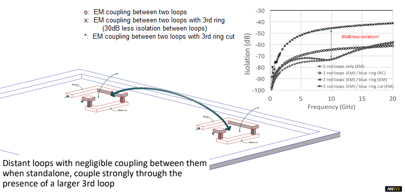
The figure above illustrates the importance of modeling this physical coupling. Two “isolated” small loops in the layout are 1mm apart and when fully extracted and analyzed together, they are quite isolated with very weak coupling. The layout also contains a third larger ring 20mm x 25mm. When the RC effects of that third bigger ring are considered, there is a minimal impact on the isolation between the two coils. However, when full electromagnetic (EM) extraction (RLCk) and analysis are performed, the graph shows that the isolation between the two small loops is reduced by 30dB at 10GHz due to the additional EM coupling. Note that the third ring/loop is not physically adjacent to the two IP loops – full electromagnetic coupling differs from the short-range of electric-field capacitive crosstalk.
(Parenthetically, to prove that the EM coupling is from the 3rd loop, an additional analysis was done with the 3rd loop “cut” – the isolation returns to the 2 loop-only results, as depicted in the figure above.)
The surrounding structures on-chip that could contribute to electromagnetic coupling include a myriad of possibilities – e.g., P/G grids (with decoupling caps), seal rings, the bulk silicon substrate, redistribution layer metals on the package, etc.
So, why are SoC EM coupling issues emerging?
The figure above illustrates that the isolation between IP blocks is impacted primarily at very high frequencies. Consider current SoC designs where a multitude of serial transceiver signal lanes are packed together on the die – for example, these SerDes lanes could be transmitting PAM-4 56Gbps signals at 7GHz. A group of lanes would share a common VCO/PLL clock source – multiple groups would be integrated to provide the total required data bandwidth. (Each group could also have multiple VCO’s within, to span a greater range of transmit frequencies.) Electromagnetic coupling contributions between multiple SerDes lanes, their P/G networks, seal ring, and package structures could result in significantly increased clock jitter (at the frequency spectrum of interest), and thus an unacceptable bit error rate.
The topologies of today’s advanced packages are a critical part of the EM coupling model, as mentioned above. The redistribution and power delivery metals in 2.5D packages (with interposer) need to be included. The unique nature of multiple stacked, thinned die in 3D packages (face-to-back or face-to-face) also requires models for EM coupling.
EM Coupling Tools and Flows
The requirement for (high-performance) SoC teams to add EM coupling analysis to their sign-off methodology necessitates new tools/flows that can assist designers with the difficult task of EM model extraction and simulation.
I recently had the opportunity to chat with Yorgos Koutsoyannopoulos, Vice President of Engineering at ANSYS about the recent EM coupling tool/flow advances available.
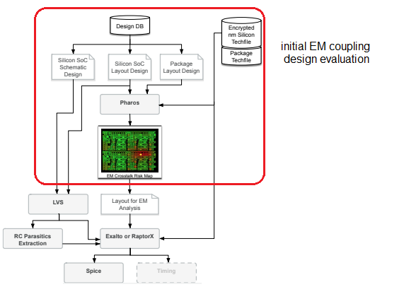
“We divided the EM coupling analysis task into two flows.”, Yorgos indicated. “The end goal is to provide designers with detailed extracted RLCk models for all relevant structures in the design, annotated to a circuit-level model for time, frequency, noise SPICE simulations. Yet, the full-chip package data volume would be unmanageable, and a large percentage of the IP signals on the SoC would not be of interest. We have developed an assessment flow to help designers pinpoint the specific nets where a detailed EM coupling model simulation is warranted.”

“How is the full chip plus package model initially generated for evaluation?”, I asked.
Yorgos replied, “The focus on the assessment flow using the ANSYS Pharos tool is to evaluate the SoC metals, vias, dielectrics, and substrate model without the circuit level detail. Designers specify the (top-level) interconnect layers of interest, and a topological model is constructed. Ports are automatically added at the physical cut points. At this juncture, without the underlying circuits, there is no annotation of an extracted RLCk model – the chip need not be LVS clean. The analysis will span the SoC IP physical hierarchy, in order to detect larger loops. The goal is to find the interacting structures that warrant further, detailed simulation.”
“What feedback is provided to the designer?”, I asked.
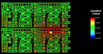
“Pharos provides both general heat maps on the excised layout database for relative visual feedback, combined with the selection of nets/grids for subsequent simulation.”, Yorgos replied. “The excised model is evaluated at a range of frequencies (and increments) provided by the designer.”

“Even with the excised SoC model, this is still a tremendous amount of physical data – what kind of IT resources are required for this early assessment?”, I inquired.
“For example, for a 100mm**2 die with the top 5 metal layers selected, the heat map for each frequency point would take roughly 1-3 hours on a 64-core 1TB memory footprint server.”, Yorgos answered. (Not too bad, I thought.)
Yorgos continued, “Pharos utilizes the same interconnect technology file as other flows – dependencies such as the metal sheet resistivity as a function of linewidth and the process corner definitions are included. For die with package models, we are able to include the package stack-up definition and redistribution layers into a unified extracted model. We also have an advanced method for modeling the die substrate into an extremely accurate RC mesh network.”
Much like design methodologies were extended to support the impact of capacitive crosstalk, it is increasingly the case that high-performance SoC IP’s (potentially utilizing advanced packaging) will need to adopt methods for broad electromagnetic coupling analysis.
To learn more about electromagnetic coupling challenges, check out this ANSYS link. Additional references with an overview of electromagnetic coupling symptoms are provided below.
-chipguy
References
[1] Ruehli, A.E., “Inductance Calculations in a Complex IC Environment”, IBM Journal of Research and Development, p. 470-481, September 1972.
[2] White, et al., “FASTHENRY: A Multipole-Acclerated 3D Inductance Extraction Algorithm”, IEEE Transactions on Microwave Theory and Techniques, Vol. 42, No. 9, p. 1750-1758, September, 1994.
[3] Restle, P., and Deutsch, A., “Designing the best clock distribution network”, VLSI Circuits Symposium, p. 2-5, 1998.
[4] Raman, A., et al., “Electromagnetic Crosstalk Failures and Symptoms in SoC Designs”, 2017 18th International Workshop on Microprocessor and SoC Test and Verification, p. 39-43.
[5] Papadopoulos, P., et al., “Challenges and Trends in SoC Electromagnetic Crosstalk”, 2017 2nd International Verification and Security Workshop (IVSW), p. 63-69.
Share this post via:


Comments
There are no comments yet.
You must register or log in to view/post comments.