There is an emerging set of advanced packaging technologies that enables unique product designs, with the capability to integrate multiple die, from potentially heterogeneous technologies. These “system-in-package” (SiP) offerings provide architects with the opportunity to optimize product performance, power, cost, and area/volume, with the capabilities to: merge processing with local memory (e.g., HBM); consolidate multiple die in rigid-substrate 2D (e.g., CoWoS) or 2.5D configurations (e.g., utilizing vertical vias through an interposer between layers); or, molding (multiple) die in a high pin count, low-cost module (e.g., FOWLP, with redistribution layers to package bumps).
In many ways, the complexities of die and advanced package technology selection are analogous to the challenges faced when targeting an integrated design to the optimum process node with appropriate PPA (and available, qualified IP).
As Moore’s Law has been consistent throughout the process generations, chip physical design methodologies have similarly evolved to help manage the increasing circuit capacity and diversity. Specifically, chip physical implementation tools transitioned from a “flat” approach to a methodology incorporating hierarchical floorplanning, interface pin constraint management, and detailed APR algorithms. Design team specializations developed, with architects working on floorplan prototypes and PD experts addressing the intricacies of routing design rules and DFM/DFY requirements.
Advanced package design shares a similar evolution – architects developing prototypes, with implementation experts completing the (bond wire or bump) die attach topologies, the signal/power routes, and the unique manufacturing patterns. SiP development tools traditionally provided a single cockpit, targeting the physical design expert – Mentor has just announced an evolution to their Xpedition product family, to address the “Moore’s Law of advanced package design flow” requirements.
I recently spoke with Keith Felton, Product Marketing Manager with the Advanced IC Packaging Solutions group at Mentor, a Siemens Business. “New tools and flows are required, to support the challenges of high-density advanced packaging, or HDAP. Mentor is introducing two new products – Xpedition Substrate Integrator and Xpedition Package Designer.”, Keith highlighted.
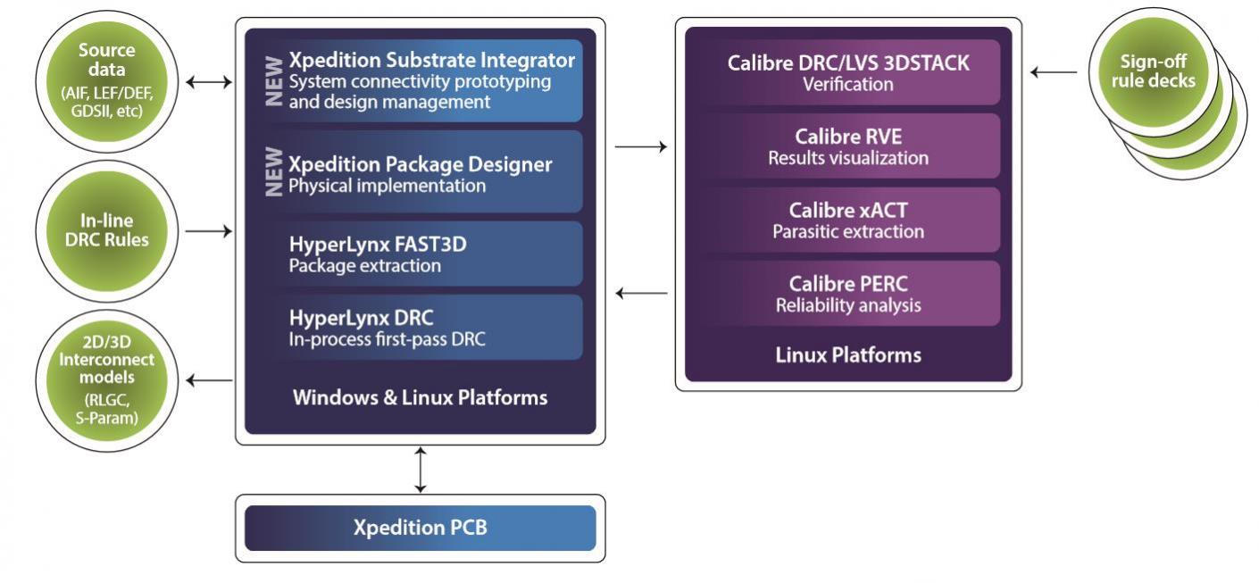
Figure 1. Xpedition Substrate Integrator and Xpedition Package Designer product positioning
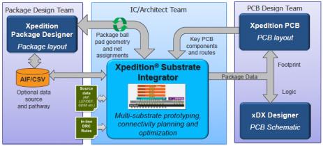
Figure 2. Design domains and data flow for xSI and xPD
“xSI is specifically targeted to support package design prototyping. The definition of the overall design connectivity is used to develop the substrate, die placement and stacking data, and preliminary bond/ball physical assignments. Architects can integrate their design concept with the PCB (using Xpedition PCB). The optimized prototype is then forwarded to the xPD flow, for final development.”, Keith explained. The figure below illustrates how a bump assignment in xSI is co-designed with the PCB, spanning the board and package domains.
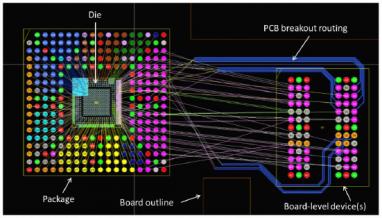
Figure 3. Data exchange between xSI and Xpedition PCB
The xSI environment integrates with HyperLynx DRC, for rule checking appropriate for initial definition (for all but the most intricate manufacturing checks). As with the hierarchical chip design flow, the architect using xSI can pass rules/constraints to detailed design – e.g., routed net shielding requirements.
Xpedition Package Designer, or xPD, is the corresponding detailed implementation tool in the new HDAP methodology. Physical design expertise finalized the attach data (bond or bump) and power/signal routes. xPD provides designers with both a 2D and (highly illustrative) 3D design view, as illustrated below.

Figure 4. 2D and 3D design views in xPD
If the prototype definition requires modification, xPD can send updates back to the xSI architect – see the double-sided flow arrow between the two tools in the flow diagram above.
The detailed design will incorporate the data appropriate for package manufacture – e.g., complex metal route and mesh fill patterns required to accommodate degassing (absorbed moisture removal at high temperature during deposition) and to minimize mechanical stress gradients in the final package. The verification of the design data will link to Mentor’s Calibre 3DSTACK, with robust algorithms/checks for the non-Manhattan geometry used in package design.
Mentor has addressed the Windows versus Linux operating system environment differences between xPD and Calibre 3DSTACK, seamlessly to designers – the correlation between Calibre and xPD data is illustrated in the figure below; full DRC and LVS checking support is provided.
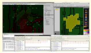
Figure 5. Xpedition Package Designer and Calibre 3DSTACK data correlation
The xPD environment also links to Mentor’s HyperLynx Fast3D algorithm for package parasitic extraction and model generation for signal integrity analysis. Mentor’s FloTHERM interfaces to xPD, as well, enabling a detailed thermal analysis of the package. Given the varying switching activity among the die and the disparate materials used (with thermal expansion coefficient differences) within the package, a thermo-mechanical stress reliability analysis is mandatory.
Chip design methodologies have evolved to support the complexities afforded by Moore’s Law, from hierarchical floorplanning to detailed DFM/DFY checks. High-density advanced packaging technology also now requires a set of tools and flows that addresses both the early design optimization space and the manufacturability/reliability requirements, leveraging the expertise of different team members. Mentor’s new Xpedition Substrate Integrator and and Xpedition Package Designer directly addresses this new package design methodology.
For more information on the new Xpedition Substrate Integrator and Xpedition Package Designer, please follow this link.
-chipguy
Share this post via:


Comments
There are no comments yet.
You must register or log in to view/post comments.