You are currently viewing SemiWiki as a guest which gives you limited access to the site. To view blog comments and experience other SemiWiki features you must be a registered member. Registration is fast, simple, and absolutely free so please,
join our community today!
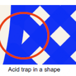
Chip designers are familiar with the additional physical design checking requirements that were incorporated into flows at advanced process nodes. With the introduction of optical correction and inverse lithography technology applied during mask data generation, and with the extension of a 193nm exposure source to finer… Read More
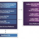
There is an emerging set of advanced packaging technologies that enables unique product designs, with the capability to integrate multiple die, from potentially heterogeneous technologies. These “system-in-package” (SiP) offerings provide architects with the opportunity to optimize product performance, power, cost,… Read More
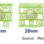
It is truly amazing to consider the advances in microelectronic process development, using 193i photolithography. The figure below is a stark reminder of the difference between the illuminating wavelength and the final imaged geometries. This technology evolution has been enabled by continued investment in mask data generation… Read More
It gives me a very nice, somewhat nostalgic, feeling after attending the 52[SUP]nd[/SUP] DAC. There was a period during my final academic year in 1990 and my first job when I used to search through good technical papers in DAC proceedings and try implementing those concepts in my project work. In general, representation from ‘R&D… Read More
One of the best things about being part of SemiWiki is the exposure to new technologies and the people behind them. SemiWiki now works with more than 35 companies and I get to spend time with each and every one of them. Much like I do, IROC Technologies works closely with the foundries and the top semiconductor companies so it was a pleasure… Read More
Yield, no topic is more important to the semiconductor ecosystem. After spending a significant part of my career on Design for Manufacturability (DFM) and Design for Yield (DFY), I’m seriously offended when semiconductor professionals make false and misleading statements that negatively affects the industry that … Read More