Automatic adaptive meshing in Ansys HFSS is a critical component of its finite element method (FEM) simulation process. Guided by Maxwell’s Equations, it efficiently refines a mesh to deliver a reliable solution, guaranteed. Engineers around the world count on this technology when designing cutting-edge electronic products. But the adaptive meshing process relies on an initial mesh that accurately represents the model’s geometry. Today, HFSS establishes the initial mesh using a suite of meshing technologies, each optimally applied to a specific type of geometry. From there, HFSS continues the adaptive refinement process until the solution converges.
Over the last two decades, computers have become larger, more powerful, and increasingly cloud-based in their high-performance computing (HPC) architecture. The FEM algorithms of HFSS have vastly improved alongside innovations in the HPC computing space. Today, they allow the rigorous and reliable simulation technology of HFSS to be applied to ever more complex electromagnetic systems. However, with larger, more complex systems, the task of initial mesh generation becomes more and more challenging.
This white paper introduces the history of HFSS meshing innovations and explores recent technological breakthroughs that have greatly improved performance and reliability in initial mesh creation.
The History of HFSS Meshing
The “Mesh” is the foundation of physics simulation; it’s how a complex modeling problem is discretized into “solvable blocks.” Understandably, for today’s highly complex systems, considerable time may be designated to generating the initial mesh because it’s such a critical step. Accurately capturing the physical geometry under test, as represented by the initial mesh, has a defining influence on the resulting simulation and speed of results. That wasn’t always the case. 25 years ago, simulation was dominated by the actual solving of the electromagnetic fields, and meshing amounted to a tiny fraction of the overall time spent generating a simulated model.
The very first HFSS simulation in 1989 took 16 hours to produce one frequency point on a then-state-of-the-art computer. The vast majority of that 16 hours was spent solving for the electromagnetic fields. Today, we can solve the same model and extract four thousand frequency points in about 30 seconds on an ordinary laptop computer. Advances in speed naturally led engineers to attempt increasingly complex designs through 3D simulation. Over the past 20 years, new meshing technologies supported the pace of innovation, but even with advanced techniques, meshing took up a larger relative portion of the process for complex designs. Simulation technologists saw that meshing was a larger pole in the “simulation tent,” so they introduced new algorithms and parallel processing to encourage further innovation in the simulation space.
Today, Ansys HFSS uses a variety of different meshing algorithms, each optimized for different geometries:
The Original “Classic”
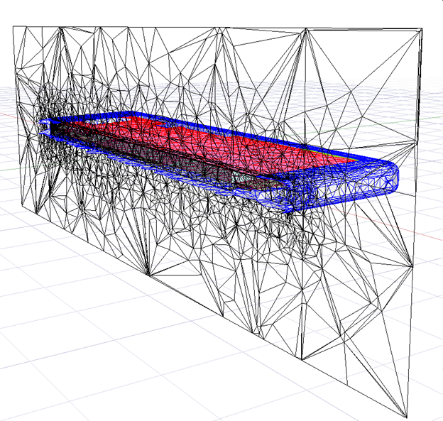
At its core, mesh generation is a space-discretization process where geometry is divided into elemental shapes. While there are several shapes to work with, in HFSS, a mesh represents geometry as a set of 3D tetrahedra, see Figure 1. It can be demonstrated that any 3D shape can be decomposed into a set of tetrahedra. Since HFSS leverages automatic mesh generation, the algorithm makes use of tetrahedra to refine and mathematically guarantee an accurate mesh.

Figure 1: Geometrically conformal tetrahedra leveraged in HFSS automatic mesh generation
Classic is one of Ansys’ earliest meshing technologies. It uses a Bowyer algorithm to create a compact mesh from any set of geometries. It’s an extremely rigorous approach. First, Classic meshes the surfaces of all objects to create a water-tight presentation of the geometry, and then it fills in the volumes of all objects with 3D tetrahedra. For accuracy, mesh elements must be continuous across a surface. In other words, two objects in contact must have a conformal triangular mesh at their adjoining faces. As geometric complexity grew and models started including hundreds or thousands of parts, it became difficult to align the triangular mesh to achieve conformal mesh everywhere. At some point, this meshing approach, which is not readily parallelized, reaches its limit. It can’t handle high levels of design complexity in a reasonable amount of time.
TAU
In 2009, Ansys released the TAU meshing algorithm. TAU approaches the task of meshing from an inverse perspective. From a bird’s-eye view, a model represents some volume of objects potentially contacting others at different points. TAU breaks up the volume into gradually smaller tetrahedra to fit each object in the model. Then, it adaptively refines and tightens local mesh size and shape to align the volumetric mesh with the faces of the input model. Eventually, TAU gets the tetrahedra close enough to each surface for a water-tight mesh that accurately represents all the geometry. For 3D CAD, such as a model of a backplane connector or an aircraft body, TAU is a very robust and reliable algorithm; however, TAU struggles with designs that include high aspect ratio geometries, like PCBs and wirebond packaging, where Classic may perform better.
Both Classic and TAU meshers are designed to handle all arbitrary geometries accurately. Depending on the model, in “Auto-mesh” mode, HFSS determines the correct mesher choice to apply.
Phi Mesher
2013 brought the next generation of meshing at Ansys—Phi. Phi is a layout-based meshing technology that’s 10, 15, or even 20 times faster than previous meshing technology, depending on the model’s geometry. A faster initial mesh often ensures faster simulations; they can be accelerated and enhanced even further with HPC.
Phi is HFSS’ first “geometry-aware” meshing technology. It relies on the layered nature of design that’s commonly found in PCBs or IC packages. The technique is based on the knowledge that all geometry in these kinds of models have a 2D layer description, with the third dimension achieved by sweeping the 2D layer description (in the XY plane) uniformly in Z. Phi was designed to accelerate initial mesh generation by conquering a 3D problem with a 2D approach. It was initially implemented in the HFSS 3D Layout design flow and eventually extended to the 3D workflow a few releases later.
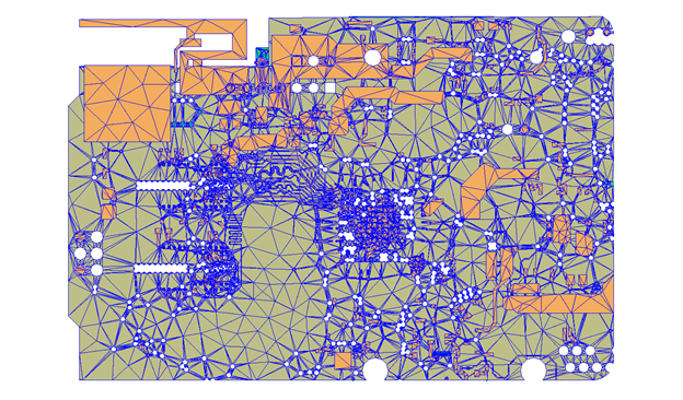
Phi performance is exceptional, achieving speeds an order of magnitude greater than other meshing technologies. In complex IC designs, see Figure 2, it’s a game changer. With earlier techniques, on-chip passive components, for example, took a considerable amount of time to complete. With Phi meshing, an hours-long initial mesh processes can be reduced to minutes or even seconds. However, Phi’s uniform-in-Z constraint limits the types of designs it can handle. For example, Phi can’t be leveraged if trace etching or bondwires were included in IC package design.

Figure 2: A typical complex PCB design, Phi mesh
That said, with the right geometry, Phi is extremely fast. Once the initial mesh is completed, the adaptive meshing algorithm works the same way as it would with any other HFSS meshing technology to produce the final convergence. In addition, Phi can create a smaller initial meshing count, which contributes to better downstream performance in the adaptive meshing and frequency sweeps. It’s faster from start to finish, not just in the initial mesh generation phase.
The Three Mesh Paradigm
With three meshing technologies in place, an Ansys auto-mesh algorithm scanned model geometries to determine which of the mesh technologies to use. In addition, fallbacks from one meshing technology to another ensured a reliable meshing flow. For example, if the algorithm identified a significant amount of high-aspect-ratio CAD, it would launch the Classic mesh algorithm. Phi was fully automated in the sense that it was always applied to uniformly swept in Z geometry.
Early on, each customer’s design flow tended to align with the same meshing techniques for every project, so they consistently gravitated to one meshing approach. However, as the HFSS solver algorithms became faster and more scalable, and cluster and Cloud hardware became more readily available, the size of HFSS simulations grew and became more complex. Designs were no longer single components; they were systems made up of multiple types of CAD. It wasn’t enough to solve just the PCB or just the connector anymore. To get it right, especially as data rates increased, it became more and more important to simulate together—connector and PCB, antenna and airframe, and so on.
As engineers design for tighter margins in the competitive electronics landscape, simulations encompass the PCB, IC packaging, connectors, surface mount components, and beyond. The Three Mesh Paradigm carried heavy burdens for customers and Ansys alike; a one-mesh-fits-all approach was not optimally effective. Understanding the different options and mesh technologies and knowing when to apply them could be a real challenge.
Enter HFSS Mesh Fusion.
The Rise of HFSS Mesh Fusion
Introduced in early 2021, HFSS Mesh Fusion achieved a fundamental meshing breakthrough using locally defined parameters. In other words, HFSS Mesh Fusion applies meshing technology depending on the local needs of the CAD. For example, when analyzing a simulation where a PCB contains both wirebond packaging and 3D connector models, such as a backplane connector, the PCB portion calls for Phi, wirebond packages call for Classic, and connectors are best meshed using TAU.
This multi-mesh capability became possible with HFSS Mesh Fusion. The only requirement is to assemble the design as a set of 3D Components, which can be encrypted to hide intellectual property and enable easy collaboration with component vendors. The 3D Component hierarchy provides the localized CAD definition to appropriately apply mesh. In addition, the same auto-mesh technology can be used to set the mesh locally, requiring little to no user input. From there, the same adaptive meshing scheme is applied to provide HFSS gold-standard accuracy and reliability.
Ansys recently worked with a team integrating a 5G chipset into a tablet computer. Before Mesh Fusion, there were a lot of mesh challenges to resolve before arriving at a usable simulation. With Mesh Fusion, Phi was applied locally to the chipset and TAU was applied to the remainder of the design—a sleek housing with complex CAD to encase the rest of the electronics in the tablet. Local mesh application ensured a clean mesh on the chipset, which was critical to the accuracy of the overall simulation. All of these seemingly disparate meshing approaches came together in Mesh Fusion for a fast, accurate, and reliable simulation result.
The Future of Meshing at Ansys
The presence of HFSS Mesh Fusion offers a night and day difference for Ansys customers. Instead of getting bogged down by meshing issues to resolve, users are free to explore more intensive design challenges that drive the electronics industry forward.
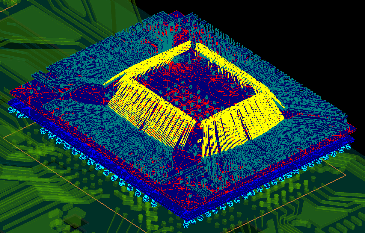
Most recently, Ansys used a ground-up approach to develop a new meshing technology. This new mesher, called Phi Plus, was designed specifically for wirebond packaging, see Figure 3., which is particularly difficult to mesh with other technologies – even Mesh Fusion. Like Phi, it’s geometry aware and takes advantage of a priori knowledge of system design. In addition, it was developed with parallelization approaches in mind, allowing for excellent scaling with HPC resources. Its success is not limited to wirebond packaging. Phi Plus can handle any kind of combined layout and 3D CAD simulation, such as connector on PCB. Phi Plus meshing is the next game changer in a long line of innovative techniques from Ansys!

Figure 3: Phi Plus Mesh applied to a wire bind package design
For updates, keep an eye on our social channels in this new year.
Also Read
The 5G Rollout Safety Controversy
Can you Simulate me now? Ansys and Keysight Prototype in 5G
Share this post via:


Comments
There are no comments yet.
You must register or log in to view/post comments.