You are currently viewing SemiWiki as a guest which gives you limited access to the site. To view blog comments and experience other SemiWiki features you must be a registered member. Registration is fast, simple, and absolutely free so please,
join our community today!
            WP_Term Object
(
    [term_id] => 24
    [name] => TSMC
    [slug] => tsmc
    [term_group] => 0
    [term_taxonomy_id] => 24
    [taxonomy] => category
    [description] =>
    [parent] => 158
    [count] => 645
    [filter] => raw
    [cat_ID] => 24
    [category_count] => 645
    [category_description] =>
    [cat_name] => TSMC
    [category_nicename] => tsmc
    [category_parent] => 158
    [is_post] =>
)

WP_Term Object
(
    [term_id] => 24
    [name] => TSMC
    [slug] => tsmc
    [term_group] => 0
    [term_taxonomy_id] => 24
    [taxonomy] => category
    [description] =>
    [parent] => 158
    [count] => 645
    [filter] => raw
    [cat_ID] => 24
    [category_count] => 645
    [category_description] =>
    [cat_name] => TSMC
    [category_nicename] => tsmc
    [category_parent] => 158
    [is_post] =>
)
Just a reminder, the semiconductor industry is doing quite well thanks to the fabless semiconductor ecosystem. TSMC, my economic bellwether, reported another great month with a 32% increase over August 2011 and a 16% increase over January-August 2011. TSMC is forecasting Q3 at a 7% increase over Q2, which was an amazing 21% increase… Read More
Reports out of Taiwan (I’m in Hsinchu this week) have TSMC more than doubling 28nm wafer output in Q3 2012 due to yield improvements and capacity increases while only spending $3.6B of the $8.5B forecasted CAPEX! Current estimates have TSMC 28nm capacity at 100,000 300mm wafers (+/- 10%) per month versus 25,000 wafers reported… Read More
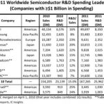
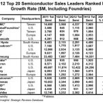
As a fitting postscript to my “Brief History of the Fabless Semiconductor Industry”, semiconductor research company IC Insights compiled a list of the top semiconductor companies for the first half of 2012. As the traditional IDMs go fabless and sink in the ratings, the foundries post record gains led by TSMC at 22%, GlobalFoundries… Read More
In 1985 Morris Chang was recruited by the Taiwanese government to help develop the emerging semiconductor industry. In 1986 Morris joined the Hsinchu based non profit research institute ITRI as Chairman and President and launched what would be TSMC’s first semiconductor wafer fabrication plant on the ITRI campus. Taiwan… Read More
Fabless semiconductor ecosystem bellwethers, TSMC and ARM, buck the trend reporting solid second quarters. Following “TSMC Reports Second Highest Quarterly Profit“, the British ARM Holdings “Outperforms Industry to Beat Forecasts“. Clearly the tabloid press death of the fabless ecosystem claims… Read More
Twenty eight nanometer is progressing very well. Our output and our yields are both above the plans that we set for ourselves and the plans that we communicated to our customers early in the year. Early in the year means January-February of the year, we set our plans in output and in yields and we, of course, ever since then we tried to… Read More
We all knew this quarter would be big but maybe not this big. Not all good news though so keep on reading. The news coverage is all over the map, mostly because they have no idea what a pure-play foundry really is. They also underestimate the power of mobile computing which should be a “Revenue by Application” market segment itself. … Read More
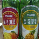
What does mango beer have to do with semiconductor design and manufacturing? At a table of beer drinkers from around the world I would have never thought fruity beer would pass a taste test, not even close. As it turns out, the mango beer is very good! Same goes for 20nm planar devices. “Will not work”, “Will not yield”, “Will not scale”,… Read More
Behind great humor often lies irony. In the midst of a struggle by the European Union to extract $1.3B from Intel in an ages old Anti-Trust case, the latter makes a strategic move to embolden the Dutch firm ASML to accelerate the development of 450mm and EUV and thus save a continental jewel. What now say EU? When disfunction and bankruptcy… Read More
Thanks to SemiWiki readers for the feedback and comments on the previous “Introduction to FinFET Technology” posts – very much appreciated! The next installment on FinFET modeling will be uploaded soon.
In the interim, Dan forwarded the following link to me “ Intel’s FinFETs too complicated and difficult, says … Read More