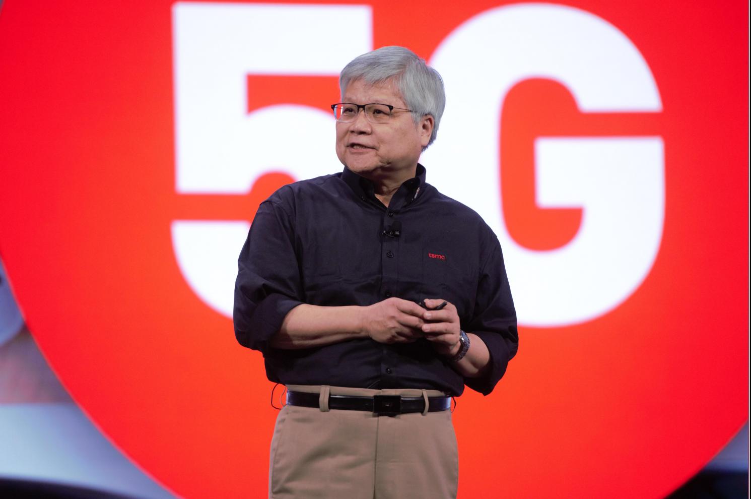
This year TSMC did a FinFET victory lap with the success of 16nm, 12nm, 10nm, and 7nm. It really is well deserved. Even though TSMC credits the ecosystem and customers, I credit TSMC and their relationship with Apple since it has pushed us all much harder than ever before. TSMC CEO C.C. Wei summed it up nicely in his keynote: Innovation,… Read More
TSMC Q1 2019 Earnings Call Discussion!
It’s no coincidence that the TSMC Symposium is right after the Q1 earnings call. This will allow TSMC to talk more freely and they certainly will, my opinion. It is a very interesting time in the semiconductor industry and TSMC, being the bellwether, can tell us what will happen the rest of the year and give us some 2020 insights.… Read More
Samsung 5nm and TSMC 6nm Update
TSMC and Samsung continue to raise the competitive bar for FinFET foundry market share with dueling announcements this week. As I mentioned previously in the blog Semiconductor Foundry Landscape Update 2019, FinFETs are the market to watch with the coming onslaught of 5G and AI chips on the edge, in the cloud, and in our autonomous… Read More
A Collaborative Driven Solution
Last week TSMC announced the availability of its complete 5nm design infrastructure that enables SoC designers to implement advanced mobile and high-performance computing applications for the emerging 5G and AI driven markets. This fifth generation 3D FinFET design infrastructure includes technology files, PDKs (Process… Read More
Semiconductor Foundry Landscape Update 2019
The semiconductor foundry landscape changed in 2018 when GLOBALFOUNDRIES and Intel paused their leading edge foundry efforts. Intel quietly told partners they would no longer pursue the foundry business and GF publicly shut down their 7nm process development and pivoted towards existing process nodes while trimming headcount… Read More
FCMN 2019 Coming up Next Month
On April 2 – 4, the 2019 International Conference on Frontiers of Characterization and Metrology for Nanoelectronics (FCMN) will be held at the Monterey Marriott in Monterey, CA. The 2019 FCMN is the 12th in the series that began in 1995 with a keynote talk by Craig Barrett, ex-CEO of Intel.… Read More
GLOBALFOUNDRIES UPDATE 2019
The GLOBALFOUNDRIES story has been one of the more interesting ones inside the fabless semiconductor ecosystem. It started in 2008 when AMD announced a partnership with ATIC of Abu Dhabi to create a new joint venture company to become the world’s first truly global semiconductor foundry. On March 4[SUP]th[/SUP] of 2009 (happy… Read More
LithoVision 2019 – Semiconductor Technology Trends and their impact on Lithography
I was asked to present at Nikon’s LithoVision event again this year. LithoVision is held the day before the SPIE Advanced Lithography Conference also in San Jose. The following is a write up of my talk.… Read More
Synopsys GLOBALFOUNDRIES and Automotive IP
IP vendors have always had the inside track on the status of new process nodes and what customers are planning for their next designs. This is even more apparent now that systems companies are successfully doing their own chips by leveraging the massive amounts of commercial IP available today. Proving once again that IP really … Read More
Physical Design for Secure Split Manufacturing of ICs
Semiconductors are not only critical to modern life, semiconductors are critical to National Security. Now that leading edge semiconductor foundries have left the United States one of the more pressing challenges is secure semiconductor manufacturing. This applies to all countries of course so let’s take a look at the International… Read More






Siemens U2U 3D IC Design and Verification Panel