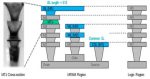
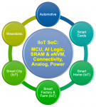
You are currently viewing SemiWiki as a guest which gives you limited access to the site. To view blog comments and experience other SemiWiki features you must be a registered member. Registration is fast, simple, and absolutely free so please,
join our community today!
WP_Term Object
(
[term_id] => 158
[name] => Foundries
[slug] => semiconductor-manufacturers
[term_group] => 0
[term_taxonomy_id] => 158
[taxonomy] => category
[description] =>
[parent] => 0
[count] => 1353
[filter] => raw
[cat_ID] => 158
[category_count] => 1353
[category_description] =>
[cat_name] => Foundries
[category_nicename] => semiconductor-manufacturers
[category_parent] => 0
[is_post] =>
)
TSMC recently held their annual Technology Symposium in Santa Clara. Part 1 of this article focused on the semiconductor process highlights. This part reviews the advanced packaging technologies presented at the symposium.
TSMC has clearly made a transition from a “pure” wafer-level foundry to a supplier of complex integrated… Read More
Each year, TSMC conducts two major customer events worldwide – the TSMC Technology Symposium in the Spring and the TSMC Open Innovation Platform Ecosystem Forum in the Fall. The Technology Symposium event was recently held in Santa Clara, CA, providing an extensive update on the status of advanced semiconductor and packaging… Read More
This year TSMC did a FinFET victory lap with the success of 16nm, 12nm, 10nm, and 7nm. It really is well deserved. Even though TSMC credits the ecosystem and customers, I credit TSMC and their relationship with Apple since it has pushed us all much harder than ever before. TSMC CEO C.C. Wei summed it up nicely in his keynote: Innovation,… Read More
It’s no coincidence that the TSMC Symposium is right after the Q1 earnings call. This will allow TSMC to talk more freely and they certainly will, my opinion. It is a very interesting time in the semiconductor industry and TSMC, being the bellwether, can tell us what will happen the rest of the year and give us some 2020 insights.… Read More
TSMC and Samsung continue to raise the competitive bar for FinFET foundry market share with dueling announcements this week. As I mentioned previously in the blog Semiconductor Foundry Landscape Update 2019, FinFETs are the market to watch with the coming onslaught of 5G and AI chips on the edge, in the cloud, and in our autonomous… Read More
Last week TSMC announced the availability of its complete 5nm design infrastructure that enables SoC designers to implement advanced mobile and high-performance computing applications for the emerging 5G and AI driven markets. This fifth generation 3D FinFET design infrastructure includes technology files, PDKs (Process… Read More
The semiconductor foundry landscape changed in 2018 when GLOBALFOUNDRIES and Intel paused their leading edge foundry efforts. Intel quietly told partners they would no longer pursue the foundry business and GF publicly shut down their 7nm process development and pivoted towards existing process nodes while trimming headcount… Read More
On April 2 – 4, the 2019 International Conference on Frontiers of Characterization and Metrology for Nanoelectronics (FCMN) will be held at the Monterey Marriott in Monterey, CA. The 2019 FCMN is the 12th in the series that began in 1995 with a keynote talk by Craig Barrett, ex-CEO of Intel.… Read More
The GLOBALFOUNDRIES story has been one of the more interesting ones inside the fabless semiconductor ecosystem. It started in 2008 when AMD announced a partnership with ATIC of Abu Dhabi to create a new joint venture company to become the world’s first truly global semiconductor foundry. On March 4[SUP]th[/SUP] of 2009 (happy… Read More
I was asked to present at Nikon’s LithoVision event again this year. LithoVision is held the day before the SPIE Advanced Lithography Conference also in San Jose. The following is a write up of my talk.… Read More
TSMC Process Simplification for Advanced Nodes