You are currently viewing SemiWiki as a guest which gives you limited access to the site. To view blog comments and experience other SemiWiki features you must be a registered member. Registration is fast, simple, and absolutely free so please,
join our community today!
WP_Term Object
(
    [term_id] => 16126
    [name] => Lithography
    [slug] => lithography
    [term_group] => 0
    [term_taxonomy_id] => 16126
    [taxonomy] => category
    [description] =>
    [parent] => 0
    [count] => 190
    [filter] => raw
    [cat_ID] => 16126
    [category_count] => 190
    [category_description] =>
    [cat_name] => Lithography
    [category_nicename] => lithography
    [category_parent] => 0
    [is_post] =>
)
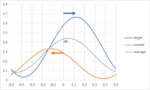
-Business will “drift down” over the course of 2023
-Not just memory is weak- China issue, foundry/logic slowing
-March guide worse than expected (Like Lam)
-Backlog likely saw push outs & cancelations but still long
Good quarter but weak guide
Much as we saw with Lam, KLA reported a beat on the December quarter… Read More
-US, Japan & Dutch agree to embargo some China chip equip
-Goes beyond just leading edge & will increase negative impact
-China might catch up in decades or invade Taiwan tomorrow
-Why the memory downturn could be longer than expected
Ganging up on China
It appears that the US has put together a coalition of the US, Japan and… Read More
For a leading-edge lithography technology, EUV (extreme ultraviolet) lithography is still plagued by some fundamental issues. While stochastically occurring defects probably have been the most often discussed, other issues, such as image shifts and fading [1-5], are an intrinsic part of using reflective EUV optics. However,… Read More
-Demand far exceeds supply & much longer than any downturn
-Full speed ahead-$40B in solid backlog provides great comfort
-ASP increase shows strength- China is non issue
-In a completely different league than other equipment makers
Reports a good beat & Guide
Revenues were Euro6.4B with system sales making up Euro4.7B… Read More
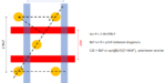
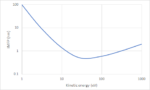
The pursuit of ever smaller DRAM cell sizes is still active and ongoing. DRAM cell size is projected to approach 0.0013 um2 for the D12 node. Patterning challenges are significant whether considering the use of DUV or EUV lithography. In particular, ASML reported that when center-to-center values reached 40 nm, single patterning… Read More
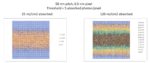
Stochastic defects in EUV lithography have been studied over the last few years. For years, the Poisson noise from the low photon density of EUV had been suspected [1,2]. EUV distinguishes itself from DUV lithography with secondary electrons functioning as intermediary agents in generating reactions in the resist. Therefore,… Read More
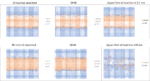
Extreme ultraviolet (EUV) lithography targets patterning pitches below 50 nm, which is beyond the resolution of an immersion lithography system without multiple patterning. In the process of exposing smaller pitches, stochastic patterning effects, i.e., random local pattern errors from unwanted resist removal or lack … Read More
The resolution of EUV lithography is commonly expected to benefit from the shorter wavelengths (13.2-13.8 nm) but in actuality the printing process needs to include Pde the consideration of the lower energy electrons released by the absorption of EUV photons. The EUV photon energy itself has a nominal energy range of 90-94 eV,… Read More
-ASML has great QTR & Outlook & Huge Euro8.9B orders
-Relatively immune from China due to mainly non leading edge
-Monster Euro38B backlog – 60EUV & 375DUV systems in 2023
-5% China risk to 2023- still mainly supply constrained
ASML proves litho’s place at Apex of semiconductor food chain
ASML announced… Read More
In spite of increasing usage of EUV lithography, stochastic defects have not gone away. What’s becoming clearer is that EUV doses must be managed to minimize the impact from such defects. The 2022 edition of the International Roadmap for Devices and Systems has updated its Lithography portion [1]. An upward trend with decreasing… Read More


Why Huawei Says It Will Match TSMC’s Most Advanced Chips by 2031