You are currently viewing SemiWiki as a guest which gives you limited access to the site. To view blog comments and experience other SemiWiki features you must be a registered member. Registration is fast, simple, and absolutely free so please,
join our community today!
WP_Term Object
(
    [term_id] => 89
    [name] => FinFET
    [slug] => finfet
    [term_group] => 0
    [term_taxonomy_id] => 89
    [taxonomy] => category
    [description] =>
    [parent] => 0
    [count] => 231
    [filter] => raw
    [cat_ID] => 89
    [category_count] => 231
    [category_description] =>
    [cat_name] => FinFET
    [category_nicename] => finfet
    [category_parent] => 0
    [is_post] =>
)
I’m a user of many Samsung products as my family has Samsung Galaxy smart phones and my MacBook Pro uses Samsung SSD for storage, so at DAC I attended a breakfast panel with presenters from Samsung, Synopsys and Qualcomm. This was the second day of DAC and they served us breakfast, and with the big names on the panel the room was… Read More
The TSMC OIP Ecosystem Forum is upon us again. I have yet to meet a disappointed attendee so it is definitely worth your time: Networking with more than 1,000 semiconductor professionals, the food, mingling with the 50+ EDA, IP, and Services Companies, the food, and of course the content. The 7nm and 7nm EUV updates alone are worth… Read More
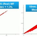
Extraction Features for 7nmby Tom Dillinger on 08-21-2017 at 12:00 pmCategories: Cadence, EDA, FinFET
Frequent Semiwiki readers are familiar with the importance of close collaboration between the foundries and EDA tool developers, to provide the crucial features required by new process nodes. Perhaps the best illustration of the significance of this collaboration is the technical evolution of layout parasitic extraction.… Read More
Traditionally, EDA has been a brute force methodology where we buy more software licenses and more CPUs and keep running endless jobs to keep up with the increasing design and process complexities. SPICE simulation for example; when I meet chip designers (which I do quite frequently) I ask them how many simulations they do for a … Read More
Experience gives us the ability to make better decisions and in a fast moving industry like semiconductors, experience is critical. As chips get more integrated and complex the number of design decisions that must be made increases at a dramatic rate. Process technologies for example, never in the history of semiconductors have… Read More
At Semicon West last week I attended presentations by Soitec and CEA Leti, and had breakfast with CEA Leti CEO Marie Semeria, key members of the Fully Depleted Silicon On Insulator (FDSOI) ecosystem. I have also seen some comments in the SemiWiki forum lately that make me believe there is some confusion on the roles of different companies… Read More
I have previously published analysis’ converting leading edge logic processes to “standard nodes” and comparing standard nodes by company and time. Recently updated details on the 7nm process node have become available and in this article, I will revisit the standard node calculations and trends.… Read More
Scott Jones and I had the opportunity to talk again with Gary Patton, GlobalFoundries CTO and SVP of R&D for a quick update on 7nm and EUV. Gary has been at GF for two years now with more than 500 other technologists from the IBM semiconductor acquisition. 7nm is the first IBM based process from GF (14nm was licensed from Samsung),… Read More
While some might have expected the exponential growth in design rules number and complexity to cool down a little, it looks as if these are only heating up more. The multiplicity of technology nodes, lithography options, , fundamental technology options (Bulk, FD-SOI, FinFET), different process flavors and specific applications,… Read More
For an industry that drives improvement at an exponential rate it is funny how often something old is new again. Intel went into high volume production on 22nm in 2011, and TSMC and Samsung have both had 20nm technologies in production for several years. And yet, recently we have seen renewed interest in 22nm. GLOBALFOUNDRIES has… Read More


Musk’s Orbital Compute Vision: TERAFAB and the End of the Terrestrial Data Center