163% Production Surge and Major Clients Help Samsung Challenge TSMC in Advanced Semiconductor Race

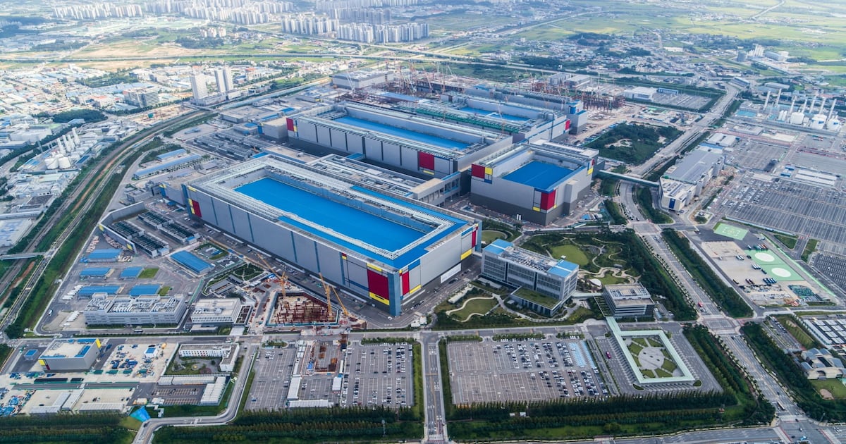
Samsung Electronics' foundry (semiconductor contract manufacturing), which had fallen significantly behind Taiwan's TSMC, has secured technological competitiveness and began to catch up.
Samsung, which initially struggled with low yields during the early adoption of its advanced 3-nanometer (1 nanometer is one-billionth of a meter) process, has recently stabilized its 3-nanometer technology and is now advancing toward narrowing the gap with TSMC by securing stability in its 2-nanometer technology. Industry observers predict that Samsung Foundry will achieve profitability starting in 2027, when the operational rate of its Taylor, Texas fab (scheduled to begin operations next year) increases, and begin a full-scale pursuit of TSMC.
◇Expanding 2-Nanometer Production
Counterpoint Research, a market research firm, projected on the 20th that Samsung Electronics' 2-nanometer production capacity will increase by 163% from 8,000 wafers per month in 2024 to 21,000 wafers by the end of next year. This expansion follows the stabilization of yield rates for Samsung's 2-nanometer process. Counterpoint Research stated, "As Samsung secures more customers in mobile, supercomputing, and AI sectors, advancements in its 2-nanometer process could serve as a critical turning point. If yield stabilization continues to improve and mass production at the Taylor fab proceeds smoothly, Samsung could meaningfully narrow the competitive gap with TSMC in leading-edge processes for the first time in several generations."
Samsung's current 2-nanometer yield rate is estimated to have risen to 55–60%. With improved yields, Samsung has successfully attracted major clients for its advanced processes. In July, it secured a US$16.5 billion (approximately 24.28 trillion Korean won) contract with Tesla to produce next-generation AI6 chips. Additionally, Samsung System LSI secured orders for its in-house smartphone application processor (AP) Exynos 2600, Apple's image sensors, and application-specific integrated circuits (ASICs) for mining from Chinese companies MicroBT and Canaan. There are also expectations that Qualcomm's AP could be added to this list.
◇Flexible Pricing Strategy to Attract Customers
According to TrendForce, a market research firm, TSMC held a dominant 70.2% share of the foundry market in the second quarter, while Samsung Electronics accounted for just 7.3%. The gap, which had narrowed to 30 percentage points in 2019, has since widened.
However, the tech industry believes Samsung could once again compete with TSMC in the 2-nanometer process. Samsung introduced the gate-all-around (GAA) transistor design in its 3-nanometer process, a technology that minimizes current leakage and significantly improves performance and power efficiency compared to the traditional fin-shaped field-effect transistor (FinFET) design. Samsung adopted GAA starting with its 3-nanometer process, while TSMC will apply it from the 2-nanometer node. A source from the tech industry remarked, "Samsung gained diverse experience with GAA while overcoming challenges in its 3-nanometer process, placing it in a different position from TSMC, which is just beginning to adopt the new technology."
Currently, TSMC faces a surge in orders from major clients like NVIDIA and Apple. Consequently, TSMC has reportedly increased the price of its 2-nanometer wafers by 50% compared to previous generations. This could benefit Samsung, which is leveraging a flexible pricing strategy to attract customers. Additionally, Samsung is focusing on securing volume by expanding its client base across various process nodes, showing signs of recovery in foundry sales. Recently, Samsung won production contracts from US AI semiconductor startups Charbright (4-nanometer), Anaplash (28-nanometer), and South Korean startup DeepX (2-nanometer). A semiconductor industry source noted, "TSMC struggles to accept new orders due to its focus on fulfilling large volumes for big tech clients like NVIDIA and Apple, while also raising wafer prices. This creates a niche market for Samsung to exploit."
◇Aiming for Profitability
The tech industry anticipates that Samsung Foundry, which has recorded quarterly losses in the billions for years, will turn profitable starting in 2027. This outlook is driven by the expected increase in operational rates at its Austin, Texas fab and the planned mass production of Tesla's AI6 chips at the Taylor fab from 2027.
During its third-quarter earnings call achieved, Samsung stated, "We record-high order intake centered on leading-edge processes, including large 2-nanometer customer orders. Alongside the full-scale mass production of new products using the 2-nanometer process, we expect further improvements in performance through continued operational rate enhancements and cost-efficiency initiatives."
 www.chosun.com
Samsung Electronics' foundry (semiconductor contract manufacturing), which had fallen significantly behind Taiwan's TSMC, has secured technological competitiveness and began to catch up.
Samsung, which initially struggled with low yields during the early adoption of its advanced 3-nanometer (1 nanometer is one-billionth of a meter) process, has recently stabilized its 3-nanometer technology and is now advancing toward narrowing the gap with TSMC by securing stability in its 2-nanometer technology. Industry observers predict that Samsung Foundry will achieve profitability starting in 2027, when the operational rate of its Taylor, Texas fab (scheduled to begin operations next year) increases, and begin a full-scale pursuit of TSMC.
◇Expanding 2-Nanometer Production
Counterpoint Research, a market research firm, projected on the 20th that Samsung Electronics' 2-nanometer production capacity will increase by 163% from 8,000 wafers per month in 2024 to 21,000 wafers by the end of next year. This expansion follows the stabilization of yield rates for Samsung's 2-nanometer process. Counterpoint Research stated, "As Samsung secures more customers in mobile, supercomputing, and AI sectors, advancements in its 2-nanometer process could serve as a critical turning point. If yield stabilization continues to improve and mass production at the Taylor fab proceeds smoothly, Samsung could meaningfully narrow the competitive gap with TSMC in leading-edge processes for the first time in several generations."
Samsung's current 2-nanometer yield rate is estimated to have risen to 55–60%. With improved yields, Samsung has successfully attracted major clients for its advanced processes. In July, it secured a US$16.5 billion (approximately 24.28 trillion Korean won) contract with Tesla to produce next-generation AI6 chips. Additionally, Samsung System LSI secured orders for its in-house smartphone application processor (AP) Exynos 2600, Apple's image sensors, and application-specific integrated circuits (ASICs) for mining from Chinese companies MicroBT and Canaan. There are also expectations that Qualcomm's AP could be added to this list.
◇Flexible Pricing Strategy to Attract Customers
According to TrendForce, a market research firm, TSMC held a dominant 70.2% share of the foundry market in the second quarter, while Samsung Electronics accounted for just 7.3%. The gap, which had narrowed to 30 percentage points in 2019, has since widened.
However, the tech industry believes Samsung could once again compete with TSMC in the 2-nanometer process. Samsung introduced the gate-all-around (GAA) transistor design in its 3-nanometer process, a technology that minimizes current leakage and significantly improves performance and power efficiency compared to the traditional fin-shaped field-effect transistor (FinFET) design. Samsung adopted GAA starting with its 3-nanometer process, while TSMC will apply it from the 2-nanometer node. A source from the tech industry remarked, "Samsung gained diverse experience with GAA while overcoming challenges in its 3-nanometer process, placing it in a different position from TSMC, which is just beginning to adopt the new technology."
Currently, TSMC faces a surge in orders from major clients like NVIDIA and Apple. Consequently, TSMC has reportedly increased the price of its 2-nanometer wafers by 50% compared to previous generations. This could benefit Samsung, which is leveraging a flexible pricing strategy to attract customers. Additionally, Samsung is focusing on securing volume by expanding its client base across various process nodes, showing signs of recovery in foundry sales. Recently, Samsung won production contracts from US AI semiconductor startups Charbright (4-nanometer), Anaplash (28-nanometer), and South Korean startup DeepX (2-nanometer). A semiconductor industry source noted, "TSMC struggles to accept new orders due to its focus on fulfilling large volumes for big tech clients like NVIDIA and Apple, while also raising wafer prices. This creates a niche market for Samsung to exploit."
◇Aiming for Profitability
The tech industry anticipates that Samsung Foundry, which has recorded quarterly losses in the billions for years, will turn profitable starting in 2027. This outlook is driven by the expected increase in operational rates at its Austin, Texas fab and the planned mass production of Tesla's AI6 chips at the Taylor fab from 2027.
During its third-quarter earnings call achieved, Samsung stated, "We record-high order intake centered on leading-edge processes, including large 2-nanometer customer orders. Alongside the full-scale mass production of new products using the 2-nanometer process, we expect further improvements in performance through continued operational rate enhancements and cost-efficiency initiatives."
Samsung Foundry Boosts 2-Nanometer Output, Eyes TSMC Gap Closure
Samsung Foundry Boosts 2-Nanometer Output, Eyes TSMC Gap Closure 163% Production Surge and Major Clients Help Samsung Challenge TSMC in Advanced Semiconductor Race