Technology typically evolves in waves. Sometimes it’s referred to as a “revolution” or an “age”. The industrial revolution and the information age are examples. These kinds of categorizations help to clarify the impact of innovation in ways that are relevant to everyone – you can’t look away if the world is changing around you.… Read More

Embedded Systems Development Flow
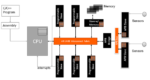
Earlier this year. as part of my coverage of the virtual Design Automation Conference (DAC), I interviewed Agnisys CEO and founder Anupam Bakshi. He talked about the new products they introduced at the show and filled me in on the history of the company and his own background. Recently, Anupam presented the webinar “System Development… Read More
I Have Seen the Future – Cornami’s TruStream Computational Fabric Changes Computing

Here is another installment regarding presentations at the Linley Fall Processor Conference. Every now and again, you see a presentation at an event like this that shakes you up. Sometimes in a good way, sometimes not so much. I attended the Cornami presentation on its new TruStream computational fabric and I was definitely shaken… Read More
Designing Smarter, not Smaller AI Chips with GLOBALFOUNDRIES

On October 20 at the Linley Fall Processor Conference, GLOBALFOUNDRIES made a compelling case for designing smarter, not smaller AI chips. The virtual conference was filled with presentations on the latest architectures and chips for all types of AI/ML applications. It was therefore a refreshing change of pace to hear the fab… Read More
Mentor User2User Virtual Event 2020!

Now that we have gone virtual, life has never been easier, for me anyway. There are literally events every day beamed into my living room. The question is which should I attend? The answer is I should attend the ones with the most customer-based content, which is what User2User is all about. I will miss attending this one live as it was… Read More
Flex Logix Brings AI to the Masses with InferX X1

In April, I covered a new AI inference chip from Flex Logix. Called InferX X1, this part had some very promising performance metrics. Rather than the data center, the chip focused on accelerating AI inference at the edge, where power and form factor are key metrics for success. The initial information on the chip was presented at … Read More
Israel and Automotive Safety. More Active Than You May Think.

CadenceLIVE ran a session recently in Europe which I thought would be interesting to check out, especially around automotive needs. The live sessions were too early/late for me (middle of the night) and sadly the talks I really wanted to hear weren’t recorded. Instead, I dug around for updates on automotive electronics in Europe.… Read More
The Most Interesting CEO in Semiconductors!
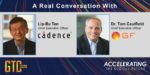
Hands down, without a doubt, the most interesting CEO in semiconductors is Lip-Bu Tan, founder of Walden Capitol and current CEO of Cadence Design Systems. If you want to talk about a man with a plan it’s Lip-Bu Tan.
Before we get into the fireside chat between Tom Caufield and Lip-Bu at the GTC 2020 Virtual event let’s do a quick biography:… Read More
Automotive Upate at Arm DevSummit from VW

Although our family has down-sized to just one vehicle, my dream car is still a Tesla, both because it’s an EV and they have a vision for autonomous vehicles. At the recent Arm DevSummit I watched a fireside chat with Alexander Hitzinger, CEO of Artemis, the skunkworks at Audi, part of the Volkswagen Group. I knew that Audi … Read More
yieldHUB – Helping Semiconductor Companies be More Competitive

The semiconductor industry is fiercely competitive. This is widely known by the SemiWiki community. When it comes to critical design parameters such as power, performance or area you’re either in the envelope that defines the market or you’re not a player. Yield management has a similar impact. Those who can stay ahead of the yield… Read More
Silicon Insurance: Why eFPGA is Cheaper Than a Respin — and Why It Matters in the Intel 18A Era