
This is the third and final blog I have written about the recent AI Hardware Summit held at the Computer History Museum in Mountain View, CA. Day 1 of the conference was more about solutions in the data center, whereas Day 2 was primarily around solutions at the Edge. This presentation from Day 2 was given by Dr. Thomas Anderson, Head, Machine Learning and AI, Design Group at Synopsys. Thomas started his presentation with an analysis of the types of AI/ML applications that are particularly difficult to implement today and how Synopsys is helping designers solve this challenge. The journey this presentation went through then got increasingly interesting.
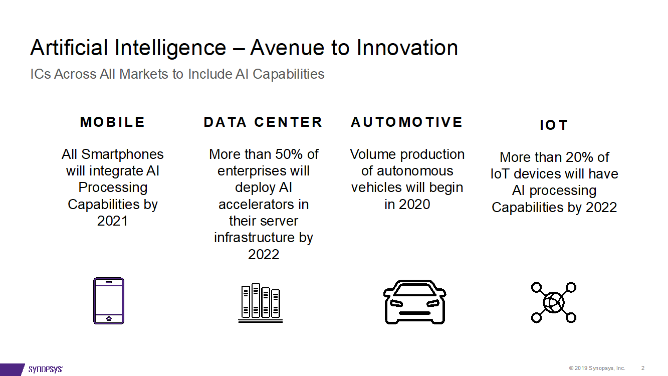
When we look at some of the current and near-future AI/ML challenges, we see huge scaling issues. Thomas pointed to the massive numbers shown in the diagram above. Granted these are challenges for the design centers, but there are similar problems at Edge as well. Next Thomas mentioned some recent breakthrough advances in AI. Thomas first pointed to Natural Language Processing, a problem that is typically solved using supervised learning, as an application that needs to be solved in a model that will run (on TPU2) with a 100ms response time. As another example, Generative Adversarial Networks uses two neural nets – one generates images and the other analyzes images – to learn how to detect fake images. AI breakthroughs are coming at a furious pace.
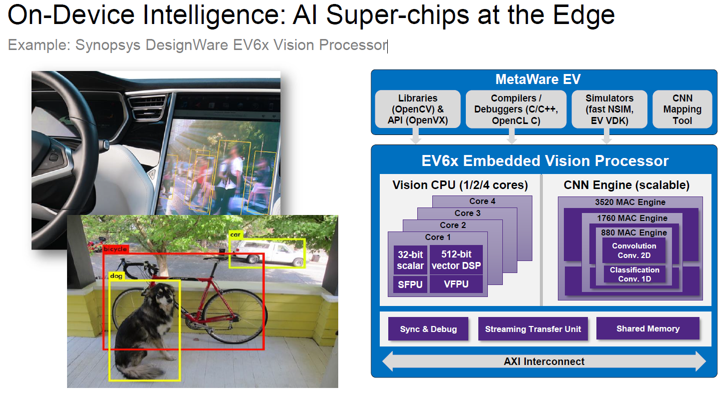
By now we have all seen the progression in AI solutions in the Cloud migrate from CPU, to GPU, and now to FPGA and application-specific processors. Synopsys EDA tools have played a large role in building these solutions. Putting together these advanced technologies for computing at the Edge is just as difficult. Synopsys support these efforts in many ways through software, tools, IP, and other advanced technologies. One example of this is the Synopsys DesignWare EV6x and EV7x Vision Processors. In a 16nm process, the EV6x convolutional neural network (CNN) engine delivers a power efficiency of up to 2,000 GMACs/sec/W, and the EV7x delivers an industry-leading 35TOPS. Both processors support a comprehensive software programming environment based on existing and emerging embedded vision and neural network standards. Using these software and hardware building blocks can save a tremendous amount of time when building your AI chip. Read more about the EV Processor family here.
The presentation by Thomas went on to discuss many other tools and the IP Synopsys has available for these types of designs. I won’t go into detail here, but Platform Architect Ultra looked like a very useful tool for architectural exploration, a topic that came up repeatedly at the summit.
Rather than go into the other tools that were discussed in the presentation, I want to take a quick look at where the conversation went next – using AI in the chip design process itself. A couple of things we know AI can do well is search a large solution space and self-training. So, the question is, “Can we train machines to build ICs?”
The AI program, AlphaGo Zero, went from zero to world champion in 40 days! It did this by teaching itself. By using a technique called reinforcement learning, the program played against itself to learn how to play better. It learned very quickly. This type of learning is quite interesting since it doesn’t rely on human knowledge or experience. Applied to chip design, we might find AI solutions that are completely different from previous human-designed chips. However, chip design is a lot more difficult than Go. According to Thomas, the estimated number of states in Go is 10360, while the number of states in a modern placement solution likely exceeds 1090,000.
So, if the design space is so huge, how can we use AI to design chips in the new future? It seems likely by using a combination of reinforcement learning along with Neural Acceleration Search and focusing on one functional design area at a time for now, likely physical design problems such as placement. This technique, Neural Acceleration Search, just announced by MIT earlier this year, provides a way to speed up learning by about 200x. While it is unlikely that AI technique will be designing entire chips from a functional specification in the next decade, we may see tremendous advances by applying AI to several chip design tasks. It is good to know that Synopsys is researching these new technology advancements from non-EDA areas to apply them to difficult EDA problems.
Share this post via:


Comments
There are no comments yet.
You must register or log in to view/post comments.