You are currently viewing SemiWiki as a guest which gives you limited access to the site. To view blog comments and experience other SemiWiki features you must be a registered member. Registration is fast, simple, and absolutely free so please,
join our community today!
WP_Term Object
(
    [term_id] => 157
    [name] => EDA
    [slug] => eda
    [term_group] => 0
    [term_taxonomy_id] => 157
    [taxonomy] => category
    [description] => Electronic Design Automation
    [parent] => 0
    [count] => 4623
    [filter] => raw
    [cat_ID] => 157
    [category_count] => 4623
    [category_description] => Electronic Design Automation
    [cat_name] => EDA
    [category_nicename] => eda
    [category_parent] => 0
    [is_post] =>
)
Imagine trying to run your EDA business only to have a competitor squat on your domain name and then make disparaging remarks about you. This sounds like a match made for reality TV however it is quite real, and now this chapter in EDA has a happy ending because Methodics can use www.methodics.com as their domain name.
The Bad Guy
We’ve… Read More
Agilent acquired EEsof back in 1999, now the EEsof group acquired Accelicon on December 1, 2011. The terms of the deal are not disclosed.
SPICE circuit simulators are only as accurate as their models and algorithms. On the model side we have Accelicon that provides EDA tools to create SPICE models based on silicon measurements:… Read More
HSPICE is over 30 years old, which is a testimony of how solid the circuit simulator has been and how widely used it is. To stay competitive the HSPICE developers have to innovate or the product will slowly loose ground to the many other simulator choices. I listened to the webinar last week to find out what was new with HSPICE.
Szekit… Read More
Earlier this week I went to the Synopsys Interoperability Forum. The big news of the day turned out to be Synopsys wanting to be more than interoperable with Magma, but that only got announced after we’d all gone away.
Philippe Margashack of ST opened, reviewing his slides from a presentation at the same forum from 10 years … Read More
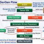
My last IC design at Intel was a Graphics Chip and I developed a layout generator for Programmable Logic Arrays (PLA) that automated the task, so I’ve always been interested in how to make IC layout more push-button and less polygon pushing. Today I watched a video about HiPer DevGen from Tanner EDA and wanted to share what I … Read More
Network-on-Chip (NoC) is an emerging paradigm for communications within large VLSI systems implemented on a single silicon chip. Sgroi et al. call “the layered-stack approach to the design of the on-chip intercore communications the Network-on-Chip (NOC) methodology.” In a NoC system, modules such as processor… Read More
Flash analog-to-digital converters (ADCs) are commonly used in high-frequency applications such as satellite communications, sampling oscilloscopes, and radar detection. Flash ADC is preferred over other ADC architectures because it is extremely fast and quite simple. However, flash ADC typically requires twice as many… Read More
David Liu receeived the Kaufman award for 2001 at the Kaufman award dinner a few weeks ago.
Or to be more formal about it:Dr. C. L. David Liu, the William Mong honorary chair professor of Computer Science and former president of the National Tsing Hua University in Hsinchu, Taiwan, will be presented with this year’s Phil Kaufman Award… Read More
Every week I receive several webinar invitations, so the recent one from Cadence about Virtuoso Multi-Mode simulation caught my fancy because I had met with John Pierce at DAC and wanted to see what was new since then and see how they compared with Mentor and Synopsys tools.
John Pierce, Product Marketing Director
This webinar runs… Read More













Why America’s Semiconductor Manufacturing Capacity Matters