
DFM closure is a growing issue these days even at the 45nm node, and IC designers at ST-Ericsson have learned that transitioning from dummy fill to SmartFill has saved them time and improved their DFM score.
The SOC
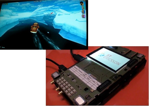
ST-Ericsson designed an SOC for mobile platforms called the U8500 and their foundry choice was a 45nm node at STMicroelectronics.

They called the chip U8500 and it had to balance battery life, graphics and a multitude of competitive features. This SOC includes:
- Single-chip base band and APE
- HSPA+ Modem Release 7
- SMP Dual ARM Cortex A9 1GHz multicore processor
- Symbian foundation, Linux Android, MeeGo and Windows Mobile OS support
- High-definition 1080p camcorder and video
- About 100 hours audio playback
- 10 hours HD video playback
- TV out using HDMI
- Video and imaging accelerators
Low power goals were achieved by using:
- Adaptive Voltage Scaling
- Dynamic voltage and frequency Scaling
- CPU Wait for Interrupts (WFI)
- RAM data retention during WFI
- Fast wake-up
- Lower power IO: HDMI, MIPI, LP DDR2, USB
DFM Closure
The fab (STMicroelectronics) at first provided standard DummyFill rules in their Calibre deck to ST-Ericsson. The result was that DummyFill didn’t meet all of the density related constraints in their process. There were two density rules not being satisfied with the DummyFill approach (fill first, verify after fill is completed).
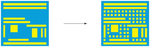
Dummy fill example where extra shapes are added to an IC layer in order to meet layout density requirements.
The second approach was to tweak the dummy fill rule deck in order to reach a DFM clean layout. Even this approach was not a complete success as shown in the following comparison table:
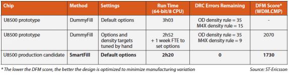
The final results in the third row of the comparison table show that using the new SmartFill capability in The Calibre YieldEnhancer tool produced a layout with 0 DRC errors and the lowest DFM score.
DummyFill adds new fill shapes across the entire chip first, then you have to run a DRC tool as a second step to see your DRC and DFM score results.
In contrast the SmartFill approach is analyzing the new fill shapes as they are being placed to make sure that they are DRC clean while meeting the fill constraints. To the EDA tool user it has now become more of a push-button approach instead of an iterative approach, you just need to make sure that your foundry process is supporting Caliber YieldEnhancer.
The U8500 SOC has 1.2 million standard cells at the top level along with 32Mbit of SRAM, so saving time in DFM closure really helped out.
Fill and Timing
Because SmartFill (or DummyFill) adds new shapes to layers the timing of an IC will be impacted. A new fill shape adds extra parasitic capacitance which in turn can impact timing results.
STMicroelectronics ran a digital test chip in their 45nm process to make some comparison measurements of the DummyFill versus SmartFill options:
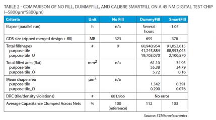
With SmartFill the table shows that the run time is close to that of DummyFill, while the GDS size got smaller, more fill shapes were created, total filled area was reduced, no DRC errors reported and the capacitance values were actually reduced.
The “purpose tile_O” shapes are the largest fill shapes and they have a higher spacing requirement between the layout and these fill shapes. Fewer of these shapes is an improvement because it creates less OPC work and helps to reduce capacitance values, which in turn means less impact on timing.
Design teams typically only re-run timing on their most critical paths after SmartFill, not re-run all static and dynamic testing.
With Calibre YieldEnhancer you can even provide a list of critical nets as an input so that SmartFill can avoid changing your timing on these nets during the fill process.
Rapid Thermal Annealing (RTA)
During semiconductor manufacturing there are thermal steps used to create shallow junctions which then affect transistor performance like: Vth (Threshold Voltage) shifts, Vth variation. The three things that contribute to RTA effects are: pattern density of the layout, the RTA temperature, and the amount of time spent in annealing. As a designer we can only impact the pattern density of the layout.
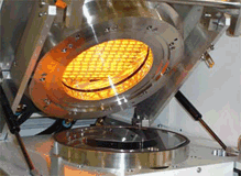
Fill shapes created by Calibre SmartFill take this into account and control the reflectivity of the wafer surface. This helps to control the electrical variability introduced by RTA.
Summary
To ensure DFM closure, maintain timing integrity and reduce variability effects at the 45nm node you should consider moving from the DummyFill approach to a SmartFill approach. ST-Ericsson and STMicroelectronics have achieved a better DFM score by using Calibre SmartFill on their U8500 SOC. More details about this topic can be found in this white paper.


Comments
0 Replies to “How ST-Ericsson Improved DFM Closure using SmartFill”
You must register or log in to view/post comments.