You are currently viewing SemiWiki as a guest which gives you limited access to the site. To view blog comments and experience other SemiWiki features you must be a registered member. Registration is fast, simple, and absolutely free so please,
join our community today!
WP_Term Object
(
    [term_id] => 157
    [name] => EDA
    [slug] => eda
    [term_group] => 0
    [term_taxonomy_id] => 157
    [taxonomy] => category
    [description] => Electronic Design Automation
    [parent] => 0
    [count] => 4231
    [filter] => raw
    [cat_ID] => 157
    [category_count] => 4231
    [category_description] => Electronic Design Automation
    [cat_name] => EDA
    [category_nicename] => eda
    [category_parent] => 0
    [is_post] =>
)
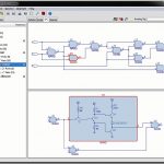
A very popular acronym is ‘WYSIWYG’ – What You See Is What You Get! This is very true and is important to visualize things to make it better in various aspects such as aesthetics, compactness, organization, structure, understandable for correction and so on; the most important, in case of semiconductor design, is being able to identify… Read More
If we look at the past, most of the EDA tools in the semiconductor design space have originated from a designers’ need to do things faster. Regardless of whether it is design exploration, manual design, simulation, verification, optimization (Power Performance Area – PPA) and many other steps in the overall design flow.… Read More
Most programmers can read a code snippet and spot errors, given enough hours in the day, sufficient caffeine, and the right lens prescription. As lines of code run rampant, with more unfamiliar third-party code in the mix, interprocedural and data flow issues become more important – and harder to spot.
Verification IP particularly… Read More
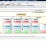
In the current semiconductor design landscape, the design size and complexity of SoCs has grown to large extent with stable tools and technologies that can take care of integrating several IPs together. With that mammoth growth in designs, verification flows are evolving continuously to tackle the verification challenges … Read More
I first started using WordPress in 2008 after having written my own Content Management System (CMS) to build and manage web sites. WordPress is the number one CMS in the world, is just 10 years old, and is used by over 70 million users. What got me thinking about WordPress and EDA software companies was a recent book by Scott Burken, … Read More
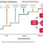
The semiconductor industry seems to be the most challenged in terms of cost of error; a delay of 3 months in product development cycle can reduce revenue by about 27% and that of 6 months can reduce it by almost half; competition is rife, pushing the products to next generation (with more functionality, low power, high performance,… Read More
IC designers have a long tradition of mixing and matching EDA tools from multiple vendors, mostly because they enjoy best-in-class tools, or they just purchased each EDA tool at a different time and asked for them to work together. Such is this case with IC layout tools from Silvacoand DRC/LVS tools from Mentor Graphics. Pawan Fangaria… Read More
There’s a French EDA company named DOCEA Powerthat is uniquely focused on power analysis at the ESL level and I had a chance to interview Ridha Hamza to get new insight on ESL design challenges and their approach. Ridha started out doing SRAM design at STMicroelectornics in the 1990’s, moved into the emerging field … Read More
Inside a today’s typical VLSI system, there are millions of electrical signals. They make the system perform what it is designed to do. Among those, the most important one is the clock signal. From an operational perspective, clock is the timekeeper of the electrical world inside the chip/system. From a structural perspective,… Read More
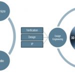
It feels to be at the top of semiconductor technology by having dies with high density of semiconductor design at sub-20nm technology node stacked together into a 3D-IC to form a complete SoC which can accommodate billions of gates. However there are multiple factors to be looked at in order to make that successful amid often conflicting… Read More


Should the US Government Invest in Intel?