You are currently viewing SemiWiki as a guest which gives you limited access to the site. To view blog comments and experience other SemiWiki features you must be a registered member. Registration is fast, simple, and absolutely free so please,
join our community today!
WP_Term Object
(
    [term_id] => 157
    [name] => EDA
    [slug] => eda
    [term_group] => 0
    [term_taxonomy_id] => 157
    [taxonomy] => category
    [description] => Electronic Design Automation
    [parent] => 0
    [count] => 4178
    [filter] => raw
    [cat_ID] => 157
    [category_count] => 4178
    [category_description] => Electronic Design Automation
    [cat_name] => EDA
    [category_nicename] => eda
    [category_parent] => 0
    [is_post] =>
)
In this age of SoCs with hundreds of IPs from different sources integrated together and working at high operating frequencies, FPGA designers are hard pressed keeping up the chip reliability from issues arising out of excessive static & dynamic IR drop, power & ground noise, electro migration and so on. While the IPs are… Read More
Cadence continues on its quest to be a top semiconductor IP supplier which is a good thing since the semiconductor world now revolves around IP. Cadence CEO Lip-Bu Tan mentioned IP 14 times during his keynote and he was followed by the president of Imagination Technologies and the CEO of recently acquired Tensilica. I was not afforded… Read More
3D TV has been all the rage over the past few years because of the added realism it offers the viewer, but there’s really not that much content that you can stream or play on a Blu-ray device. Wouldn’t it be cool if there was a box that could create 3D on the fly from a 2D stream or Blu-ray? This week I discovered that such a box… Read More
Jasper at DVCon and EJUGby Paul McLellan on 03-13-2014 at 7:05 pmCategories: EDA
The Jasper European User Group meeting (EJUG) is coming up in a couple of weeks. It will be held in the Munich Hilton (which I have stayed in many times, the S-bahn from the airport pretty much stops in the basement) on April 2nd.
The schedule for the day is:
9:00 AM – Registration and continental breakfast
9:30 AM – Jasper… Read More
The biggest market for semiconductors is mobile and an ARM processor is the center of the axle around which it revolves. So everyone in the mobile ecosystem needs to work closely with ARM. At CDNLive earlier this week Cadence and ARM announced that they are deepening their partnership. Most of what they announced makes it a lot easier… Read More
Wearables are going to be a real game changer for the fabless semiconductor ecosystem, absolutely. What other high volume semiconductor market segment has such a low barrier of entry? Speaking of low barrier of entry, the first stop on my Southern California trip last week was Monrovia, the home of Tanner EDA. Tanner is already … Read More
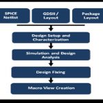
A very popular acronym is ‘WYSIWYG’ – What You See Is What You Get! This is very true and is important to visualize things to make it better in various aspects such as aesthetics, compactness, organization, structure, understandable for correction and so on; the most important, in case of semiconductor design, is being able to identify… Read More
If we look at the past, most of the EDA tools in the semiconductor design space have originated from a designers’ need to do things faster. Regardless of whether it is design exploration, manual design, simulation, verification, optimization (Power Performance Area – PPA) and many other steps in the overall design flow.… Read More
Most programmers can read a code snippet and spot errors, given enough hours in the day, sufficient caffeine, and the right lens prescription. As lines of code run rampant, with more unfamiliar third-party code in the mix, interprocedural and data flow issues become more important – and harder to spot.
Verification IP particularly… Read More
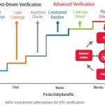
In the current semiconductor design landscape, the design size and complexity of SoCs has grown to large extent with stable tools and technologies that can take care of integrating several IPs together. With that mammoth growth in designs, verification flows are evolving continuously to tackle the verification challenges … Read More


Facing the Quantum Nature of EUV Lithography