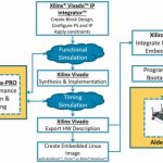
Designers tend to put tons of energy into pre-silicon verification of SoCs, with millions of dollars on the line if a piece of silicon fails due to a design flaw. Are programmable logic designers, particularly those working with an SoC such as the Xilinx Zynq, flirting with danger by not putting enough effort into verification?… Read More
Electronic Design Automation
Solido Saves Silicon with Six Sigma Simulation
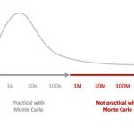
When pushing the boundaries of power and performance in leading edge memory designs, yield is always an issue. The only way to ensure that memory chips will yield is through aggressive simulation, especially at process corners to predict the effects of variation. In a recent video posted on the Solido website, John Barth of Invecas… Read More
Are Your Transistor Models Good Enough?
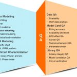
SoC designers can now capture their design ideas with high-level languages like C and SystemC, then synthesize those abstractions down into RTL code or gates, however in the end the physical IC is implemented using cell libraries made up of transistors. Circuit designers use simulation tools like SPICE on these transistor-level… Read More
Semi execs look at IoT tradeoffs a bit differently
What happens when you get a panel of four executives together with an industry-leading journalist to discuss tradeoffs in IoT designs? After the obligatory introductions, Ed Sperling took this group into questions on power, performance, and integration.… Read More
Rigid-Flex Cabling is Cool! (and requires unique EDA support)
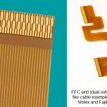
The three F’s of electronic product development are: form, fit, and function. Although the F/F/F assessment typically refers to the selection of the right component, it most definitely also refers to the selection of the proper cabling between assemblies. The requirements for cables are varied, and demanding: ability… Read More
Catching low-power simulation bugs earlier and faster
I’ve owned and used many generations of cell phones, starting back in the 1980’s with the Motorola DynaTAC phone and the biggest usability factor has always been the battery life, just how many hours of standby time will this phone provide and how many minutes of actual talk time before the battery needs to be recharged… Read More
Keynote: Silicon is the New Steel: Building the World’s First Terascale Network
Prof. Thomas Lee from Stanford University is the keynote speaker at the upcoming 38th EOS/ESD Symposium (September 11-16, Anaheim). The EOS/ESD Symposium is focused on discussing the issues and providing the answers to electrostatic discharge in electronic production and assembly.
Abstract:
Steel transformed civilization… Read More
Webinar Alert – Helping Mixed Signal not be Mixed Up
Today’s profound statement: “don’t fall in love with your tools, figure out the biz process change first.” Mixed-signal SoC designers are having ample challenges with their design process and are in need of design management, but don’t want another tool to do it.… Read More
A Software Company Making Hardware
I’ve been a daily Facebook user for many years now and it keeps me in touch with family, friends, some business contacts and even a handful of high-tech companies. My first impression is that Facebook is a very successful, cloud-based, social platform staffed with software developers and a few marketing mavens. On closer… Read More
Custom layout productivity requires unrelenting EDA vendor focus
The EDA tools industry relies upon ongoing productivity enhancements to existing products, to manage increasing SoC complexity and to address shrinking design schedules. The source of ideas for enhancements can come from a variety of sources – e.g., customer feedback, collaboration with the foundries, and features found … Read More





Musk’s Orbital Compute Vision: TERAFAB and the End of the Terrestrial Data Center