You are currently viewing SemiWiki as a guest which gives you limited access to the site. To view blog comments and experience other SemiWiki features you must be a registered member. Registration is fast, simple, and absolutely free so please,
join our community today!
WP_Term Object
(
    [term_id] => 157
    [name] => EDA
    [slug] => eda
    [term_group] => 0
    [term_taxonomy_id] => 157
    [taxonomy] => category
    [description] => Electronic Design Automation
    [parent] => 0
    [count] => 4380
    [filter] => raw
    [cat_ID] => 157
    [category_count] => 4380
    [category_description] => Electronic Design Automation
    [cat_name] => EDA
    [category_nicename] => eda
    [category_parent] => 0
    [is_post] =>
)
Many years ago, there were attempts to (re-) introduce a graphical entry approach to building RTL design. The Renoir product was one example. The idea has some initial appeal. You describe the behavior in a small block using (textual) RTL but the larger structure of instances and higher-level connectivity can be described as a … Read More
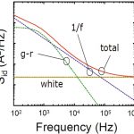
AMS and RF IC designers have known for years that their circuits are sensitive to noise, because if you amplify noise on an input source to an amplifier circuit then your chip can start to produce wrong answers. Even digital SoC designers need to start taking notice because every SoC is filled with SRAM IP blocks, and at each shrinking… Read More
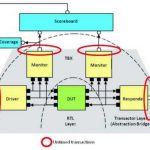
Teams buy HDL simulation for best bang for the buck. Teams buy hardware emulation for the speed. We’ve talked previously about SCE-MI transactors as a standardized vehicle to connect the two approaches to get the benefits of both in an accelerated testbench – what else should be accounted for?… Read More
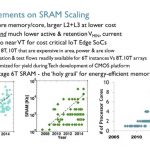
ARM’s Azeez Bhavnagarwala recently gave a talk hosted by Solido on the benefits of variation aware design in optimizing 6T bit cells. Azeez sees higher clock rates, increasing usage of SRAM per processor and the escalating number of processors, shown in the diagram below, as trends that push designers toward 6T. Six Transistor… Read More
Power is Everything
During Apollo 13 after the oxygen tank in the service module exploded forcing the crew to use the lunar module as a life boat to get back home, John Aaron – an incredibly gifted NASA engineer who was tasked with getting the Apollo 13 crew back home safely – flatly stated “Power is everything…we’ve… Read More
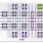
Designing DRAMs at Intel back in the 1970s I first learned about Soft Errors and the curious effect of higher failure rates of DRAM chips in Denver, Colorado with a higher altitude than Aloha, OR. With the rapid growth of FPGA-based designs in 2016, we are still asking the same questions about the reliability of our chips used for safety-critical… Read More
Israel has a strong pedigree in functional verification. Among others, Verisity (an early contributor to class-based testbench design and constrained random testing) started in Israel and RocketTick (hardware-based simulation acceleration), acquired more recently by Cadence, is based in Israel. So when I hear about an … Read More
A few weeks ago we previewed a Synopsys webinar describing how they are linking the ARM Juno Development Platform with the HAPS-80 and HAPS ProtoCompiler environment. I’ve had a look at the archived event and have some additional thoughts.… Read More
Integrated wafer-level fanout (WLFO) packaging technology is emerging as a foundation for multi-die solutions. Mobile product applications require focus on both aggressive chip-to-chip interface performance, as well as the final package volume. Traditional multi-chip packages using PCB laminate substrates do not readily… Read More
The Automotive IC market is not the largest segment, but is certainly the segments expected to grow with the highest CAGR, with 10.8% from 2013 to 2018, according with IC Insights (January 2015). If you consider the pretty long concept/design to production cycle time (7 years or more) as well as the numerous segments just emerging… Read More


Musk’s Orbital Compute Vision: TERAFAB and the End of the Terrestrial Data Center