You are currently viewing SemiWiki as a guest which gives you limited access to the site. To view blog comments and experience other SemiWiki features you must be a registered member. Registration is fast, simple, and absolutely free so please,
join our community today!
The market opportunities for machine learning hardware are becoming more succinct, with the following (rather broad) categories emerging:
- Model training: models are evaluated at the “hyperscale” data center; utilizing either general purpose processors or specialized hardware, with typical numeric precision of 32-bit
…
Read More
Package Reliability Issues Cost Moneyby Tom Dillinger on 11-13-2019 at 6:00 amCategories: Ansys, Inc., EDA
Advanced packaging technology is enabling “More Than Moore” scaling of heterogeneous technology die. At the recent EDPS Symposium in Milpitas, Craig Hillman, Director of Product Development, DfR Solutions, at ANSYS gave a compelling presentation, “Reliability Challenges in Advanced Packaging”. The key takeaway messages… Read More
The introduction of 5G communications support offers tremendous potential across a broad spectrum of applications (no pun intended). 5G is indeed quite encompassing, across a wide range of frequencies – the figure below illustrates the common terminology used, from low-band, mid-band (“sub 6G”), and high-band (“mmWave”)… Read More
High-Speed PHY IP for Hyperscale Data Centersby Tom Dillinger on 09-25-2019 at 10:00 amCategories: EDA, Synopsys
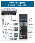
A new designation has recently entered the vernacular of the computing industry – a hyperscale data center. The adjective hyperscale implies the ability of a computing resource to scale corresponding to increased workload, to maintain an appropriate quality of service.
The traditional enterprise data center is often characterized… Read More
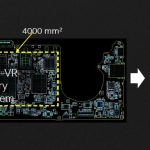
In the old days, product architects would throw a functional block diagram “over the wall” to the design team, who would plan the physical implementation, analyze the timing of estimated critical paths, and forecast the signal switching activity on representative benchmarks. A common reply back to the architects was, “We’ve… Read More
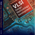
Daniel Nenni was gracious enough to encourage me to conduct a brief webinar describing a new reference text, recently published by Prentice-Hall, part of the Semiwiki Webinar Series.
VLSI DESIGN Methodology Development Webiner Replay
Background
I was motivated to write the text to provide college students with a broad background… Read More
The pace of Moore’s Law scaling for monolithic integrated circuit density has abated, due to a combination of fundamental technical challenges and financial considerations. Yet, from an architectural perspective, the diversity in end product requirements continues to grow. New heterogeneous processing units are being… Read More
SiP is the new SoC @ 56thDACby Tom Dillinger on 06-19-2019 at 6:48 pmCategories: Cadence, EDA, Events
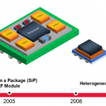
The emergence of 3D packaging technology has been accompanied by the term “more than Moore”, to reflect the increase in areal circuit density at a rate that exceeds the traditional IC scaling pace associated with Moore’s Law. At the recent Design Automation Conference in Las Vegas, numerous exhibits on the vendor floor presented… Read More
Executives from the major EDA companies attend the Design Automation Conference to introduce new product features, describe new initiatives and collaborations, meet with customers, and participate in lively conference panel discussions. Daniel Nenni and I were fortunate to be able to meet with Joe Sawicki, Executive Vice… Read More
Custom SRAM IP @56thDACby Tom Dillinger on 06-14-2019 at 8:00 pmCategories: Events, IP, sureCore
The electronics industry strives to continuously introduce new product innovation and differentiation. The ASIC market arose from the motivation to offer unique (cost-reduced) integration that was not realizable with commodity MSI/LSI parts. The SoC market evolved to provide even greater differentiation, integrating… Read More







Agentic AI Demands More Than GPUs