
Advanced packaging technology is enabling “More Than Moore” scaling of heterogeneous technology die. At the recent EDPS Symposium in Milpitas, Craig Hillman, Director of Product Development, DfR Solutions, at ANSYS gave a compelling presentation, “Reliability Challenges in Advanced Packaging”. The key takeaway messages from his talk were:
-
- Package reliability analysis is often not considered during (initial) product development – “It does not always have a seat at the table.”, in Craig’s words.
- Package reliability issues uncovered during product qualification cost BIG money. (more on that shortly)
Further, the rapid adoption of 2.5D and 3D heterogeneous packaging and the corresponding end target applications have exacerbated these issues. These issues are more pronounced due to a combination of new materials, plus the extended thermal environments and required lifetimes of emerging markets.
Specifically, Craig highlighted two failure mechanisms that merit detailed modeling and simulation – dielectric cracking/delamination within the die, and fatigue/failure of the solder connections from die to package and package to PCB.
- Low-K Dielectric Failure
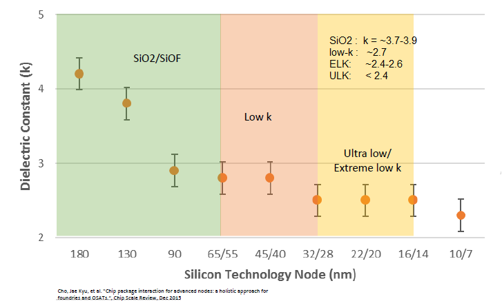
For several process nodes, the interlevel dielectrics (ILD) between back-end-of-line (BEOL) metal layers have been utilizing a “low k” material (k being the standard nomenclature for the relative dielectric constant).
These dielectric materials typically utilize plasma-enhanced chemical vapor deposition of an organosilicate glass (OSG) or spin-coating of silicon glass in a gel-based solvent. This dielectric is then etched to create the vias and metal trenches for the damascene copper metal deposition. More recently, extreme low-k (ELK) and ultra low-k (ULK) materials have been incorporated into BEOL process modules.
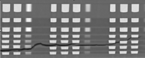
The porosity of these ELK and ULK dielectrics is greater. Correspondingly, the strain energy release rate is less. In other words, these brittle materials are more prone to catastrophic cracking due to applied stress. Fracture mechanics of materials includes both adhesive and cohesive analysis – adhesive is related to disparate material interfaces and cohesive is related to a fracture within the material itself. Craig presented data indicating a greater susceptibility for cohesive ELK/ULK cracking within the dielectric layer, as illustrated below.
The figure below highlights an additional factor in the susceptibility of these new ILD materials to fracture. The technology for die attach is transitioning from (lead-free) solder bumps to copper pillars, to provide tighter pad pitch and greater current density. However, copper has a higher modulus of rigidity than solder.
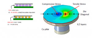
As the package is subjected to thermal events, the Cu pillar transfers more mechanical stress into the ILD materials in the die than would a solder attach metallurgy. As illustrated in the figure above, the interaction between (flip-chip) die, Cu pillar, underfill, and package substrate results in a complex combination of compressive and tensile forces on the ILD dielectric layers at the die edge, due to differences in the coefficient of thermal expansion (CTE).
Craig mentioned two additional mechanisms of interest related to dielectric fractures.
residual and applied stress
The fabrication and attach processes themselves likely result in some degree of residual stress in the ILD materials. The thermal cycling of the part is thus an interaction between this initial material stress and the thermally-generated applied stress described above. “The existing JEDEC qualification standards for thermal cycling (and temperature rate of change) may not necessarily be the worst case stress extremes.”, Craig indicated. “There are potentially ranges other than -40C to 125/150C that would be preferable. If the initial residual stress relaxes at high temperature, that could counteract the applied stress from material CTE differences. Maybe -40C to <<125C would result in greater effective stress on the dielectrics.”
propagation of initial dielectric cracks
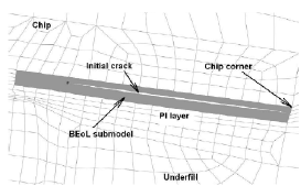
The probability and rate at which an ILD fracture results in a failure is increased significantly in the presence of an initial crack at the die edge, such as could arise during the process steps for individual die singulation from the wafer. The figure below illustrates a cross-sectional finite-element mesh model for the die, top-surface overcoat, and package attach underfill materials with an initial crack present.
Craig expanded further upon these issues, “In addition to the ELK/ULK materials transition, packaging technology has also been evaluating new underfill materials. The goal would be to utilize a material whose rigidity is less at high temperatures, to reduce the stress on the ILD. Yet, these polymers have an intricate modulus of rigidity and CTE relation as a function of temperature that could aggravate rather than reduce the applied stress. To further complicate the analysis, the Cu pillar and solder bump materials are subject to “work hardening”, where plasticity may reduce over time, due to repeated (limited) deformation occurring during thermal cycles.”
What has been the industry cost of reliability failures due to ELK/ULK cracking?
“Easily in the billions of dollars.”, Craig noted. “At ANSYS, we’ve recently had 9 companies approach us seeking a simulation analysis solution to ILD cracking issues.”
How can the risk of ELK fracture be reduced?
Craig indicated, “There are (foundry and OSAT) design rules that are intended to mitigate the risk. For example, the Cu pillar and top-level pad dimensions and spacing attempt to balance the desire for a high I/O density with the stresses transferred to the ILD layers. Adhering to metal density/uniformity requirements on top-level interconnects, especially under the pad metal is also key. And, the foundry will provide stringent guidelines for the (minimum) number of metal layers of different thicknesses in the overall interconnect stack – the process module for each metal layer has corresponding ILD features. The number and location of low-k, ELK/ULK transitions in the stack is a crucial design consideration. Yet, even with these design guidelines, the best solution to ELK/ULK reliability analysis is a thorough thermal-mechanical simulation of the material stackup, using a platform such as ANSYS Multiphysics.”
- solder fatigue
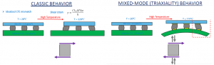
Craig also briefly reviewed another, more well-known, reliability issue, related to the fracture of solder joint connections between the package and the board. “Existing models of the strain applied to the solder joint are proving to be inadequate – companies are reporting a greater and earlier failure rate than predicted.”, Craig indicated.
“The classical 2D, planar approach to the analysis of CTE mismatch between package and board needs to be expanded. Boards are subject to their own stresses, from the (dual-sided) component placement to the mechanical attachment to the product housing. A tri-axial 3D application of stresses to solder joints is required for fatigue analysis.” The figure below illustrates the contribution to solder joint stress from board deformation.
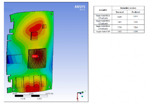
“Again, extensive simulation modeling and analysis is required of this thermal-mechanical system, even down to the torque applied to the screws that attach the boards to the standoffs in the housing.” The figure below shows an ANSYS simulation result – the color index on the board illustrates the degree of (Z-axis) deformation, while the table illustrates simulated versus measured solder joint fracture data in terms of allowed thermal cycles.
Craig concluded his presentation with the following commitment, “ANSYS is extending its Multiphysics scripting and material property modeling features to enable simulation of all artifacts that contribute to these package reliability failure modes.” That was encouraging to hear – deferring reliability analysis to product qualification is increasingly a significant financial risk.
Here’s a link to Craig’s EDPS presentation slides – link.
Here’s a link to more information on ANSYS Multiphysics – link.
-chipguy
Share this post via:


Comments
There are no comments yet.
You must register or log in to view/post comments.