You are currently viewing SemiWiki as a guest which gives you limited access to the site. To view blog comments and experience other SemiWiki features you must be a registered member. Registration is fast, simple, and absolutely free so please,
join our community today!
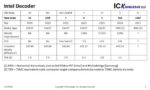
Intel presented yesterday on their plans for process technology and packaging over the next several years. This was the most detailed roadmap Intel has ever laid out. In this write up I will analyze Intel’s process announcement and how they match up with their competitors.
10nm Super Fin (SF)
10nm is now in volume production in three… Read More
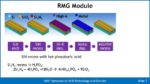
At the 2021 VLSI Technology Symposium, Imec presented on Ruthenium (Ru) and Molybdenum (Mo) as alternate Word Line (WL) materials for 3D NAND Flash “First Demonstration of Ruthenium and Molybdenum Word lines Integrated into 40nm Pitch 3D NAND Memory Devices”. I had an opportunity to interview one of the authors: Maarten Rosmeulen.… Read More
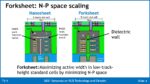
FinFETs devices are reaching their limits for scaling. Horizontal Nanosheets (HNS) are a type of Gate All Around (GAA) device that offers better scaling and performance per unit area. HNS is the logical next step from FinFETs because HNS processing is similar to FinFETs with a limited number of process changes required.
At the … Read More
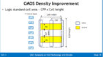
At the 2021 Symposium on VLSI Technology and Circuits in June a short course was held on “Advanced Process and Devices Technology Toward 2nm-CMOS and Emerging Memory”. In this article I will review the first two presentations covering leading edge logic devices. The two presentations are complementary and provide and excellent… Read More
IBM has announced the development of a 2nm process.
IBM Announcement
What was announced:
- “2nm”
- 50 billion transistors in a “thumbnail” sized area later disclosed to be 150mm2 = 333 million transistors per millimeter (MTx/mm2).
- 44nm Contacted Poly Pitch (CPP) with 12nm gate length.
- Gate All Around (GAA), there are several ways
…
Read More
After I published a recent article about Intel, I was contacted by the Irish Development Agency (IDA) where Intel has a large fab presence and asked if I would like to interview them about the Intel site. The interview with Turlough McCormack of the IDA, started with Intel’s presence in Ireland but then went on to paint an interesting… Read More
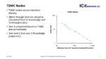
TSMC recently announced plans to spend $100 billion dollars over three years on capital. For 2021 they announced $30B in total capital with 80% on advanced nodes (7nm and smaller), 10% on packaging and masks and 10% on “specialty”.
If we take a guess at the capital for each year, we can project something like $30B for 2021 (announced),… Read More
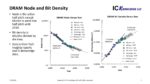
At the SPIE Advanced Lithography Conference in February 2021, Regina Freed of Applied Materials gave a paper: “Module-Level Material Engineering for Continued DRAM Scaling”. Applied Materials provided me with the presentation and was kind enough to set up an interview for me with Regina Freed.
I also spoke to Regina Freed last… Read More
There are a lot of articles out right now discussing a possible IPO for Kioxia or sale of the company with Western Digital (WD) and Micron Technology (MT) mentioned as possible acquirers. Kioxia and WD have a partnership for Flash Memory and on March 18th WD gave a presentation on the state of their partnership and what they see as their… Read More
In January I presented at the ISS conference a comparison of Intel’s, Samsung’s and TSMC’s leading edge offerings. You can read a write-up of my presentation here.
With the problems going on at Intel, that article generated a lot of interest in the investment community, and I have been holding a lot of calls with analysts who are trying… Read More


TSMC CoWoS versus Intel EMIB Semiconductor Packaging