You are currently viewing SemiWiki as a guest which gives you limited access to the site. To view blog comments and experience other SemiWiki features you must be a registered member. Registration is fast, simple, and absolutely free so please,
join our community today!
At the 2010 DACI moderated a panel session on SPICE and Fast SPICE circuit simulation, and one of the panelists was PierLuigi Dagliofrom STMicroelectronics. To get an update on SPICE circuit simulation at ST I read a PDF document at Mentor titled: Improving the Quality of SPICE Simulation Results with Eldo Premier at ST.
ST does … Read More
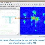
I read two blogs this week that got me to thinking about contingencies in SoC implementation. By contingency I mean using an EDA tool flow from the leading vendor for logic synthesis and then discovering that you cannot route the design without expanding the die size after a few weeks of concerted effort, then having to come up with… Read More
EDA tools come in all sizes and price ranges, so I was pleased to readthat Tanner EDAhas completed an integration with Incentia. A few months ago Tanner announced their integration with Aldec for digital simulation, and today’s announcement extends their tool suite to include digital synthesis and static timing. Here’s… Read More
After a show like DesignConwraps up we get a chance to ask ourself what it all meant, and how was this year different than last year. Reading through many posts about DesignCon I came to discover that the Awards at DesignCon are less contentious than at CES, and also that ANSYSreceived a DesignVision awardfor the 2nd year running. … Read More
The most exciting EDA + Semi IP company that I ever worked at was Silicon Compilers in the 1980’s because it allowed you to start with a concept then implement to physical layout using a library of parameterized IP, the big problem was verifying that all of the IP combinations were in fact correct. Speed forward to today and our… Read More
In the 1990s, software developers were established users of software configuration management (SCM) tools such as open source RCS/CVS or of commercial systems such as Clearcase. Hardware designers, however, managed design data in ad hoc home-grown ways. ClioSoft’s founder, Srinath Anantharaman, recognized that hardware… Read More
My oldest son just upgraded Smart Phones from a 3″ display to a 4.5″ display and was shocked to discover that his battery barely lasted 8 hours, so I welcomed him to the reality of limited battery life in modern SoC-based mobile devices. There is some hope in increasing battery life for our consumer-oriented devices … Read More
SoC designers have always wanted to simulate hardware and software together during new product development, so one practical question has been how to trade off performance versus accuracy when creating an early model of the hardware. The creative minds at Carbon Design Systems and ARM have combined to offer us some hope and relief… Read More
DesignConis next week in Santa Clara, so today I spoke with Mark Ravenstahlfrom ANSYS to get an idea of what to expect at the conference and trade show.
… Read More
Non-volatile memory is used in a wide variety of consumer and industrial applications and comes in an array of architectures like Serial Flash and CBRAM (Conductive Bridging RAM). I caught up with Shane Hollmer by phone this week to gain some insight into a recent acquisition of Atmel’s serial flash components, and how that… Read More


Why Huawei Says It Will Match TSMC’s Most Advanced Chips by 2031