You are currently viewing SemiWiki as a guest which gives you limited access to the site. To view blog comments and experience other SemiWiki features you must be a registered member. Registration is fast, simple, and absolutely free so please,
join our community today!
Introduction
IC designs go through a layout process and then a verification of that layout to determine if the layout layer width and spacing rules conform to a set of manufacturing design rules. Adhering to the layout rules will ensure that your chip has acceptable yields.
At the 28nm node a typical DRC (Design Rule Check) deck will… Read More
Introduction
Here in the Silicon Forest (Oregon) we have a venture-backed, fabless analog semi company called Avnera that has designed over 10 Analog System on Chips (ASoC). Their chips are used in consumer products for both wireless audio and video applications.
James Rollins is the director of physical design at Avnera… Read More
Introduction
Circuit designers work at the transistor level and strive to get the ultimate in performance, layout density or low power by creating crafty circuit topologies in both schematics and layout. Along with this quest comes the daunting task of verifying that all of your rules and best practices about reliability have… Read More
Inroduction
In the early days we made paper plots of an IC layout then measured the width and length of interconnect segments with a ruler to add up all of the squares, then multiplied by the resistance per square. It was tedious, error prone and took way too much time, but we were rewarded with accurate parasitic values for our SPICE… Read More
Intro
Earlier this month I drove to Mentor Graphics in Wilsonville, Oregon and spoke with Michael Buehler-Garcia, Director of Marketing and Nancy Nguyen, TME, both part of the Calibre Design to Silicon Division. I’m a big fan of correct-by-construction thinking in EDA tools and what they had to say immediately caught my… Read More
Intro
On Friday I talked with Srinath Anantharaman by phone to gain some perspective on Hardware Configuration Management (HCM) versus Software Configuration Management (SCM), especially as it applies to the IC design flows in use today. In the 1990’s we both worked at Viewlogic in Fremont, CA and in 1997 Srinath founded… Read More
Last week I met with Joseph Davis, Ph.D. at Mentor Graphics in Wilsonville, Oregon to learn about a new product designed for full-custom IC layout designers to improve productivity.
The traditional flow for full-custom IC layout designers has been nearly unchanged for decades:
- Read a schematic or use Schematic Driven Layout
…
Read More
For IC designers creating full-custom or AMS designs there are plenty of challenges to getting designs done right on the first spin of silicon. Let me give you a sneak peek into what’s being discussed at the EDA Tech Forum in Santa Clara, CA on March 10th that will be of special interest to you:
3D TSV (Through Silicon Vias) are… Read More
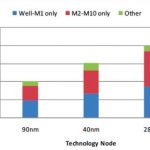
When I worked at Intel as a circuit design engineer I could talk directly with the technology development engineers to understand how to really push my DRAM designs and get the smallest possible memory cell layout that would still yield well, provide fast access time, and long refresh cycles.
(United States Patent 6661699. Inventor:… Read More
Cadence at DesignCon 2011
I met with Rahul Deokar, Product Manager this morning to review 9 slides that tell the story of Giga-gates and GigaHz systems design at Cadence. Their updated P&R system now completes jobs 2X faster for 28nm designs.
Silicon Realization Trends and Challenges:
Silicon Realization – end to end digital… Read More


Enhancing Multi-Domain System Simulation with FMI Co-Simulation