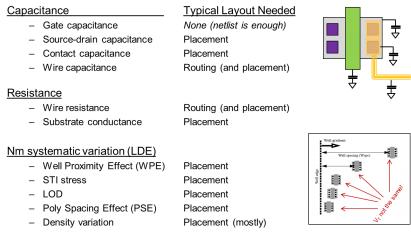
As analog and mixed-signal designers move to very advanced geometries, they must grapple with more and more complex considerations of the silicon. Not only do nanometer CMOS devices have limitations in terms of analog-relevant characteristics such gain and noise performance, but they also introduce new sources of variation which designers must worry about. Industry efforts like the TSMC AMS Reference Flow 2.0 have devoted considerable focus to this.
Managing the effects of variation has been part of analog design since the vacuum tube era. However, nanometer CMOS introduces variations that depend not only on the devices themselves, but also where they are physically located on the chip relative to one another. These new context-sensitive effects, such as well proximity, shallow trench isolation stress, and poly spacing effects, make accurate assessment of the layout’s electrical impact – also a time-honored analog design imperative – even more important. Or as the co-founder of a major fabless IC company once said, “at nanometer geometries, the layout is the schematic.”

Perhaps the biggest problem for computer analysis of these effects turns out not to be actually modeling them, but getting timely access to layout data. Because layout traditionally is a tedious and change-resistant effort, project teams don’t like to start it until the circuit design is nearly complete. Yet before the circuit design is complete – while it’s still evolving and flexible – is exactly when you do want the layout data. The layout really is just another view of the schematic.
In order to solve this Catch-22, it’s important to look at a couple of factors: how much layout is really needed for analysis? And how much of it can be automated?
For example, only placement is needed in order to assess the impact of well proximities; however, that placement needs to be accurate and complete – not just each differential pair or current mirror in isolation. Whereas routing is essential for node capacitance – but approximate routing might be adequate, especially if the capacitance is dominated by source-drain loading, in which case the wires themselves add little.

Fortunately there’s a group of companies bringing to market innovative solutions that focus exactly on these problems, and collaborating to hold the nanometer Circuit Verification Forum (nmCVF), on September 22nd at TechMart in Santa Clara. Hosted by Berkeley Design Automation, and including technologists from selected EDA, industry and academic partners, this forum will showcase advanced nanometer circuit verification technologies and techniques. You’ll hear real circuit case studies, where these solutions have been used to verify challenging nanometer circuits, including data convertors; clock generation and recovery circuits (PLLs, DLLs); high-speed I/O, image sensors and RFCMOS ICs.


The Intel Common Platform Foundry Alliance